Method and system for semiconductor design hierarchy analysis and transformation

a technology of design hierarchy and semiconductors, applied in the field of method and system for semiconductor design hierarchy analysis and transformation, can solve problems such as adding complexity to these methods

Active Publication Date: 2006-04-06
CADENCE DESIGN SYST INC
View PDF14 Cites 25 Cited by
  • Summary
  • Abstract
  • Description
  • Claims
  • Application Information

AI Technical Summary

Problems solved by technology

In many cases this is not directly amenable for design corrections or other analyses or modifications that are able to leverage the hierarchy of the design since the cell hierarchy could be very deep or cells could have significant overlap with each other.
Invariably, these need to be accommodated during the RET and OPC steps, for example, which can be an added complexity to these methods.
The design correction problem is to analyze the hierarchy and find a reasonable representation of the original design that facilitates the design correction, makes use of repeating patterns, and enables distribution of the work across a cluster of central processing units (CPU's) or on a shared memory multi-CPU machine.

Method used


Image

  • Method and system for semiconductor design hierarchy analysis and transformation
  • Method and system for semiconductor design hierarchy analysis and transformation
  • Method and system for semiconductor design hierarchy analysis and transformation

Examples


Embodiment Construction

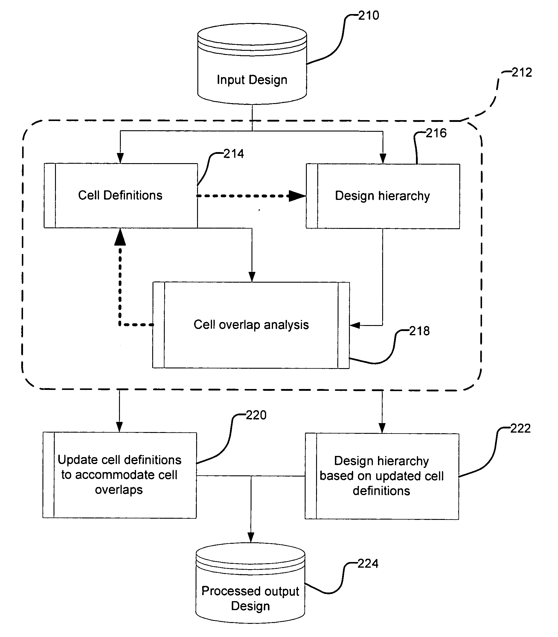
[0041]FIG. 1 illustrates the method for modifying cells in a hierarchical integrated circuit design that embodies principles of the present invention.

[0042] In more detail, processing begins at a node A in step 110. Initially this is the root node, which later become a current node as the process traverses the design.

[0043] In one embodiment, if there is no top cell, a common top cell is created and all cells are referenced into that top cell.

[0044] Next, in step 112, it is determined whether or not the node A is a leaf cell. A leaf cell has only polygons and no references to other cells.

[0045] If it is a leaf cell, then further processing is stopped in step 114.

[0046] If, however, the current node A is not a leaf cell, then it is determined whether or not any polygons are defined in node A in step 116.

[0047] If there are polygons, then a new cell(s) is created for these polygons and a reference is provided to this new cell within current node A in step 118. Typically, the num...


PUM


Abstract

A method and apparatus for partitioning of the input design into repeating patterns called template cores for the application of reticle enhancement methods, design verification for manufacturability and design corrections for optical and process effects is accomplished by hierarchy analysis to extract cell overlap information. Also hierarchy analysis is performed to extract hierarchy statistics. Finally template core candidates are identified. This allows to the design to be made amenable for design corrections or other analyses or modifications that are able to leverage the hierarchy of the design since the cell hierarchy could otherwise be very deep or cells could have significant overlap with each other.

Description

BACKGROUND OF THE INVENTION [0001] The process of fabricating integrated circuits typically involves a functional design step, followed by a physical design step. During the functional design step, a design concept is described using a hardware description language and is then converted into a netlist, which specifies the electronic components and the connections between the components. The physical design step specifies the placement of the electrical components or elements on the chip and routing of the connections between the electrical components thereby implementing the netlist. The physical design process generates the physical design data, which are synonymously called layout data, layout, or target layout. [0002] The target layout defines a set of binary patterns or objects, which are also called “features” or “geometric features”. Usually the objects are represented as a polygon or collection of polygons in the layout data in order to facilitate the specification of the obj...

Claims


Application Information

Patent Timeline
Patent Type & Authority Applications(United States)
IPC IPC(8): G06F17/50G06F9/455
CPCG06F17/5068G06F30/39
Inventor KAMAT, VISHNU GOVIND
Owner CADENCE DESIGN SYST INC
Why Eureka
Try Eureka