

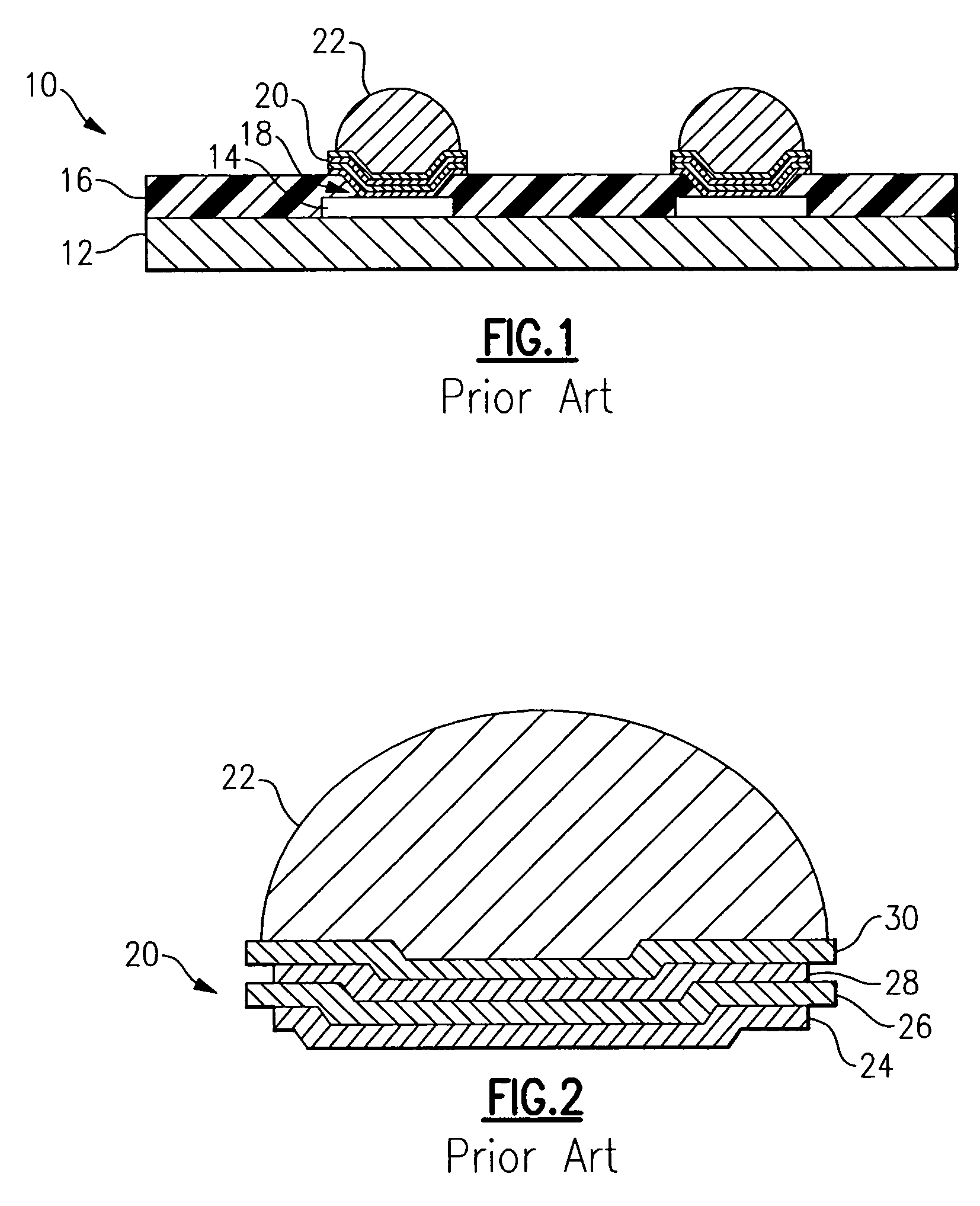
Resist sidewall spacer for C4 BLM undercut control
a sidewall spacer and undercutting technology, applied in the direction of electrical apparatus, semiconductor devices, semiconductor/solid-state device details, etc., can solve the problems of compromising the reliability of the package, requiring additional steps, and one or more blm layers undercutting the solder bump, so as to prevent preventing the undercutting of blm layers, and effectively widening the footprint of the solder bump
- Summary
- Abstract
- Description
- Claims
- Application Information
AI Technical Summary
Benefits of technology
Problems solved by technology
Method used
Image

Examples
first embodiment
[0033] As seen in FIG. 11, the present invention departs from conventional processing after the thick layer of resist 32 has been applied over BLM structure 22, as seen in FIG. 6. Instead of using conventional mask 34, a half-tone mask 46 that, in addition to having a non-transmissive region 38 in alignment with bonding pads 14 and vias 18, includes a fully transmissive region 48 surrounding non-transmissive region 38 and a partially transmissive region 50 surrounding fully transmissive region 48. After exposure to light 36 and developer, the negative resist 32 is completely removed in areas in alignment with the non-transmissive region 38, and resist 32 is partially removed in the areas in alignment with the partially transmissive region 50.
[0034] As seen in FIG. 12, etching after exposure using half-tone mask 46 leaves protective sidewalls 52 surrounding bump cavity 40. Non-transmissive region 38 of half-tone mask 46 should be dimensioned to leave sidewalls 52 having a width of ap...
second embodiment
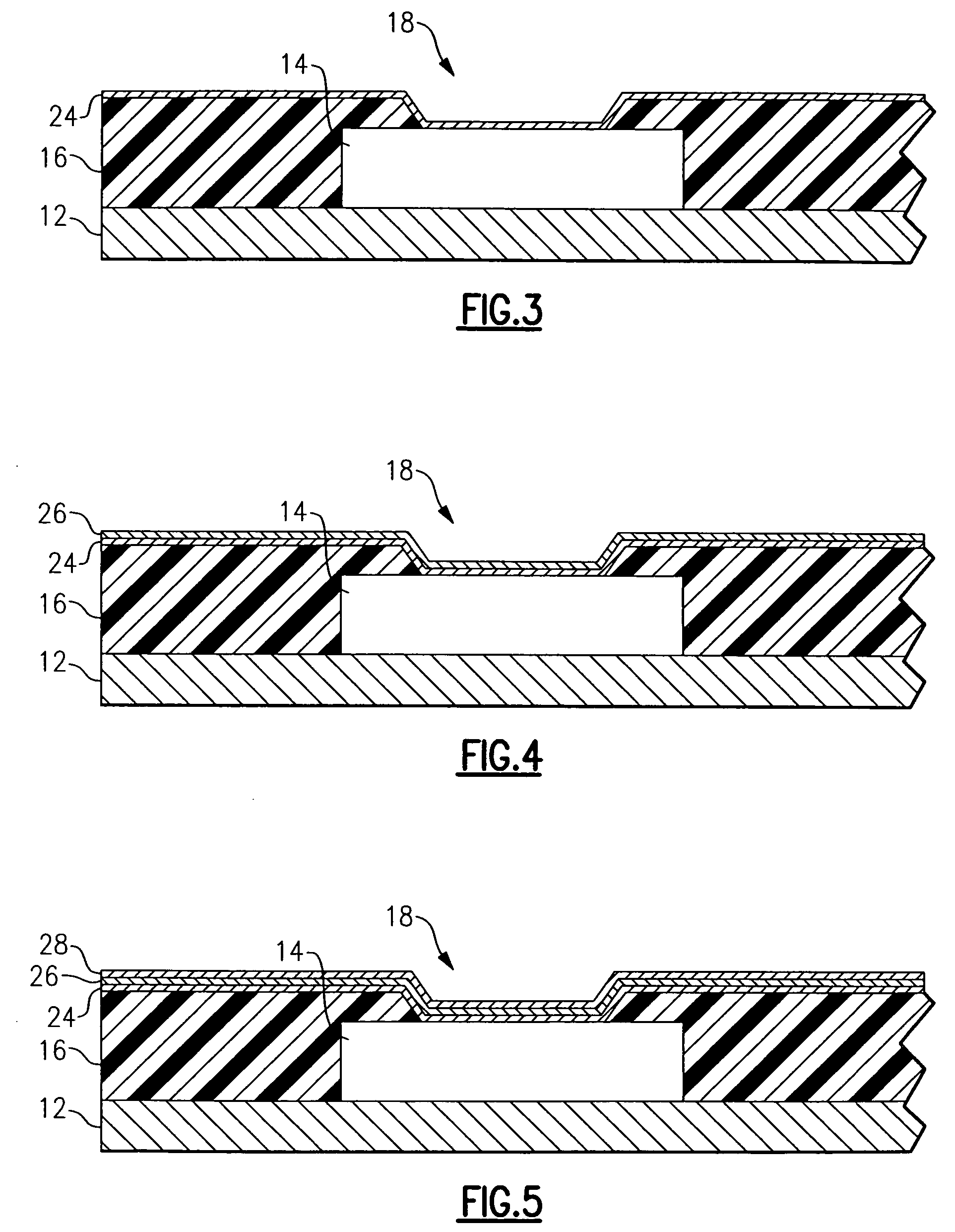
[0036] Referring to FIG. 15, the present invention comprises the conventional preparation of device 10 to include a first resist layer 32 that is masked and etched to form a cavity 40, as shown in FIGS. 6-8. Nickel barrier 42 is deposited in cavity 40 and a second resist 60 is applied over first resist 32. A mask 62 that has non-transmissive regions 64 in alignment with first resist 32 surrounding and adjacent to cavity 40 is used to expose second resist 60. After etching second resist 60, solder 44 is deposited into cavity 40. Subsequent etching removes all first resist 32 in field regions 54, leaving barriers 56 surrounding solder 44 and nickel 42. As seen in FIGS. 18-19, barriers 56 prevent undercutting of solder 44 when BLM structure 20 is etched. As seen in FIG. 20, all resist 32 is removed and solder 44 is annealed to form solder bump 22.
third embodiment
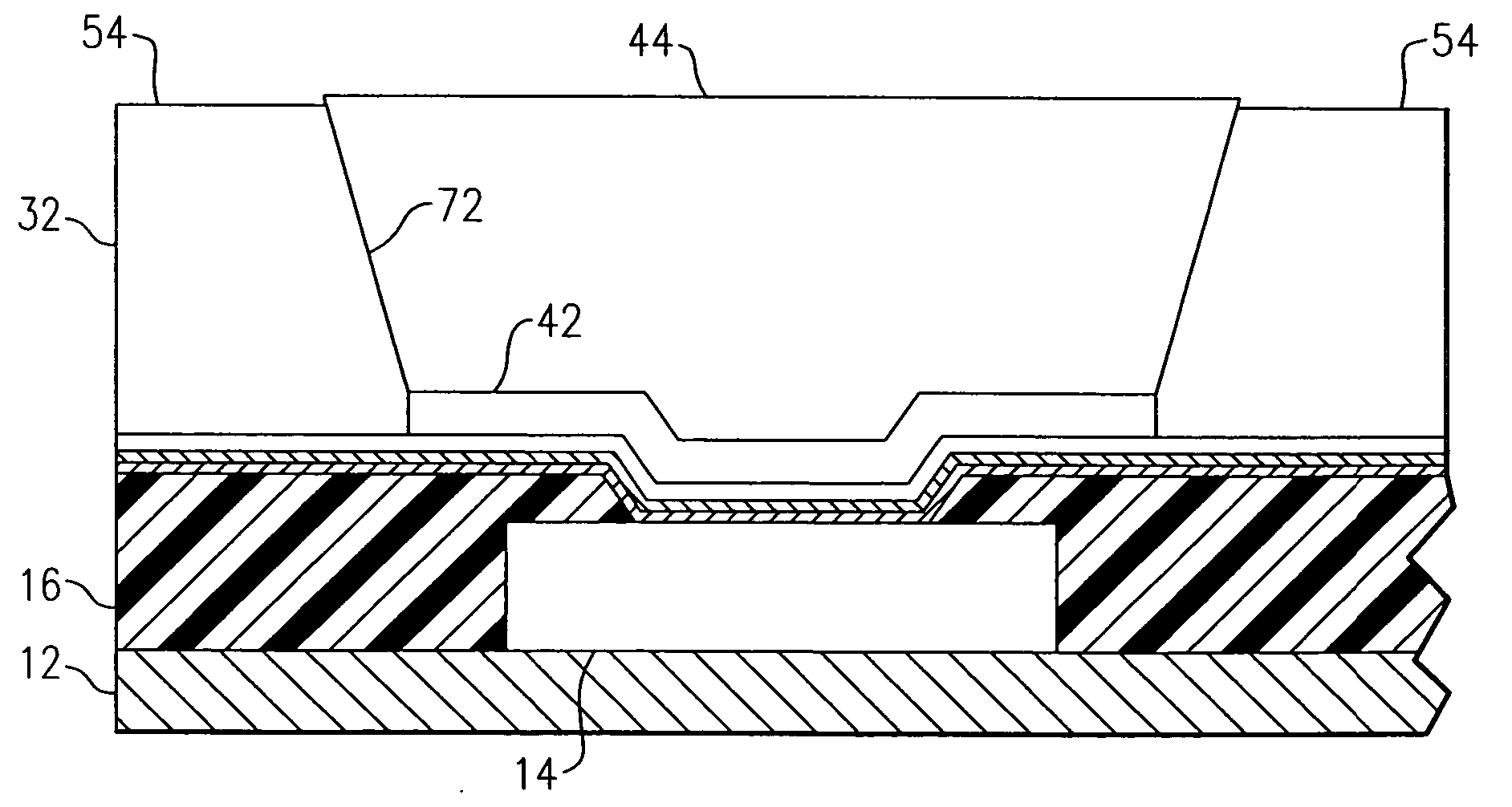
[0037] Referring to FIG. 21, the present invention comprises a conventional formation of device 10 including a first resist layer 32 and a C4 cavity 40 formed therein. A nickel barrier 42 is deposited in cavity 40 and solder 44 is plated into cavity 40 over nickel 42. A second resist 66 is then applied over first resist layer 32 and solder 44. Second resist 66 is patterned by a mask 66 containing a non-transmissive region 68 that is in alignment with solder 44 and extends outwardly to include an extended perimeter portion 70 for inhibiting etching of resist 32 in sidewalls 54 directly surrounding solder 44. After etching, protective barrier 56 surrounding solder 44 is left. As explained above, barrier 56 prevents undercutting of solder 44 when BLM structure 20 is wet etched. All resist 32 is removed and solder 44 is annealed to form solder bump 22, as seen in FIG. 20.
PUM
 Abstract
Description
Claims
Application Information