Printed wiring board, information processing apparatus, and method of manufacturing the printed wiring board

Inactive Publication Date: 2006-04-13
KK TOSHIBA
View PDF6 Cites 15 Cited by
  • Summary
  • Abstract
  • Description
  • Claims
  • Application Information

AI Technical Summary

Benefits of technology

[0011] It is an object of the present invention to provide a printed wiring board, an information processing apparatus, and a method of manufacturing the printed wiring board, which can keep manufacturing costs low and realize stable transmission of signals.
[0014] According to the present invention, it is possible to provide a printed wiring board, an information processing apparatus, and a method of manufacturing the printed wiring board, which can keep manufacturing costs low, and realize stable transmission of signals.

Problems solved by technology

However, in the case of the printed wiring board described in the above-document, since a rectangular shape of the printed wiring board needs to be cut down and hauled out from a parent material being an insulating layer in a state having an angle with respect to the direction of fiber, much of the parent material is left as scrap, which poses a problem in terms of manufacturing costs.
On the other hand, when a printed wiring board which obtains an insulating layer from prepreg and the like is used as a controlling board which requires high speed data transmission, the following problem becomes apparent: the transmission characteristics of the signals carried by wiring patterns deteriorate in a printed wiring board having a ground layer and a plurality of wiring patterns for signal transmission positioned facing to the ground layer while sandwiching a fiber-containing insulating layer.
Accordingly, impedance in the extending direction of the wiring pattern (transmitting direction of signal) differs between the former wiring pattern and the latter wiring pattern, which creates differences in signal transmission speed or signal noise.

Method used


Image

  • Printed wiring board, information processing apparatus, and method of manufacturing the printed wiring board
  • Printed wiring board, information processing apparatus, and method of manufacturing the printed wiring board
  • Printed wiring board, information processing apparatus, and method of manufacturing the printed wiring board

Examples


first embodiment

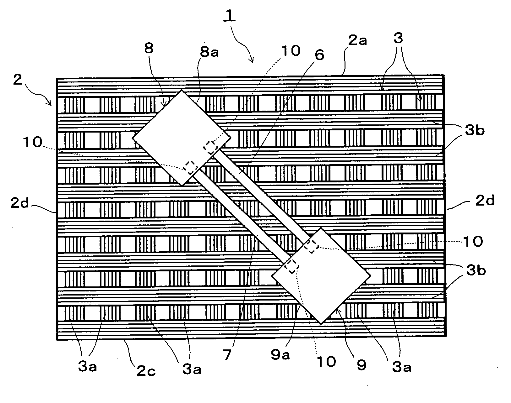
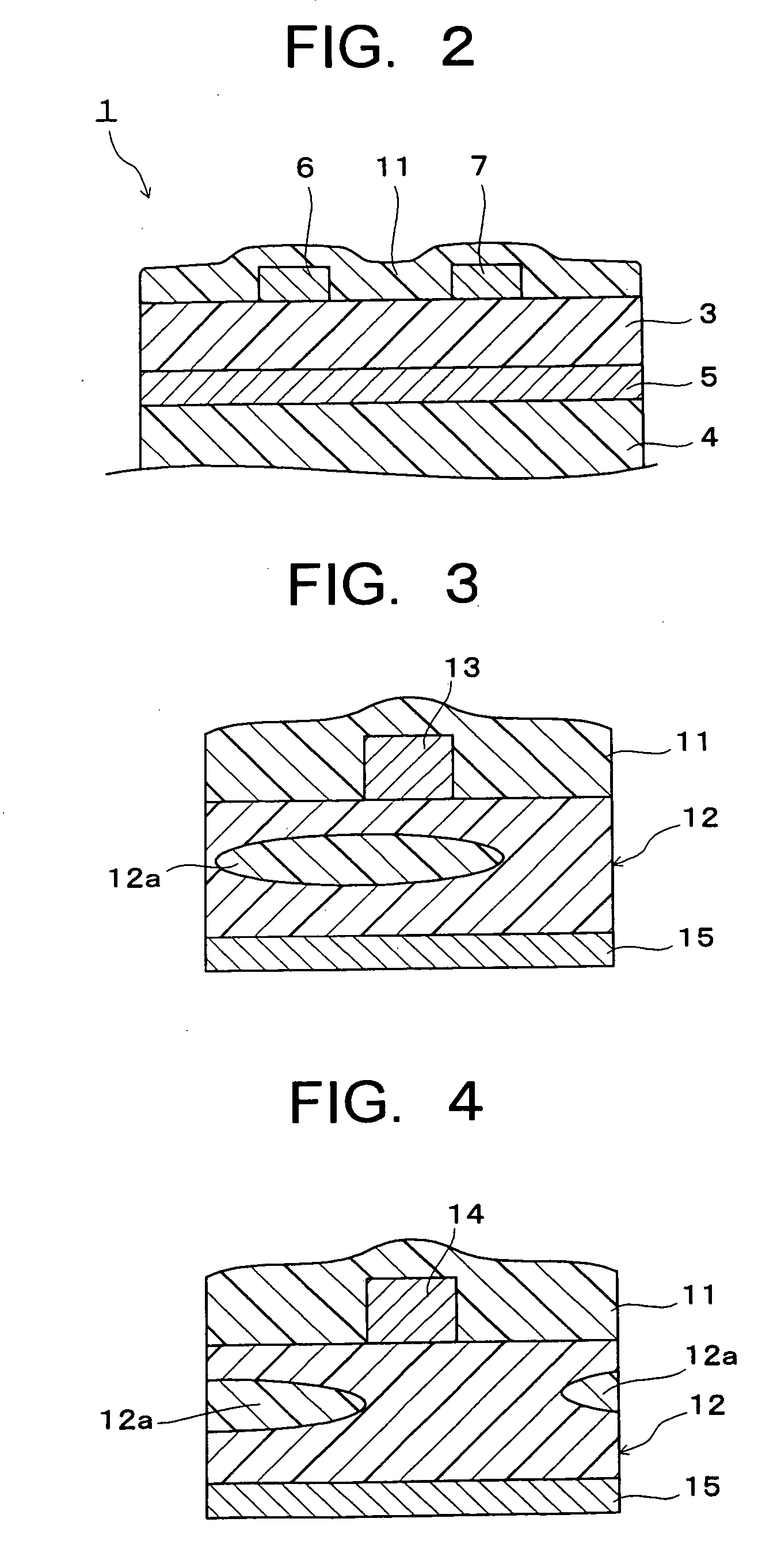
[0027]FIG. 1 is a plan view schematically showing a state that a semiconductor package is mounted on a printed wiring board according to a first embodiment of the present invention, and FIG. 2 is a sectional view of the printed wiring board shown in FIG. 1 (the semiconductor package is not shown). Here, in order to make the internal formation of this printed wiring board clear, FIG. 1 illustrates its structure in perspective.

[0028] As shown in FIGS. 1 and 2, the printed wiring board 1 is a multi-layered substrate having a plurality of conductive layers, and is composed of a substrate body 2 having a rectangular appearance. The substrate body 2 of the printed wiring board 1 includes insulating layers 3 and 4, a ground (GND) layer 5 which is an example as a reference potential layer, a plurality of wiring patterns 6 and 7 for signal transmission, and a plurality of pad sections 10 to solder-mount rectangular semiconductor packages 8 and 9 on the substrate body 2.

[0029] The above-des...

second embodiment

[0040] A second embodiment of the present invention will be explained based on FIG. 7 next. Here, FIG. 7 is a sectional view showing a printed wiring board of the second embodiment. A printed wiring board 31 according to this embodiment is a modification of the structure of the printed wiring board 1 explained in the first embodiment in a peripheral structure of a pad portion on the surface layer of the substrate body.

[0041] That is, this printed wiring board 31 is provided with a plurality of via holes 34, inside which a conductive substance 33 is filled, as vertical conductive sections right under pad portions 35. Thereby, the conductive substance 33 electrically connects to the pad portions 35. On the pad portions 35; the semiconductor package 8 (or 9) is mounted via solder bumps 36. The via hole 34 may be a non-feed through via hole connecting between a middle conductive layer inside the substrate and a conductive layer on the surface layer, or it may be a full feed through via...


PUM

PropertyMeasurementUnit
Angleaaaaaaaaaa
Angleaaaaaaaaaa
Electrical conductoraaaaaaaaaa

Abstract

Disclosed is a printed wiring board comprising an insulating layer having a rectangular flat shape and provided with fibers in the layer, the direction of the fiber in the layer being almost parallel to any side of the rectangle, a reference potential layer disposed on one surface side of the insulating layer, a plurality of wiring patterns for signal transmission disposed on the other surface side of the insulating layer so as to have nearly similar angles respectively with respect to the direction of the fiber in the insulating layer, and a pad portion to mount a semiconductor device, disposed on the other surface side of the insulating layer to conduct the plurality of wiring patterns.

Description

CROSS-REFERENCE TO THE INVENTION [0001] This application is based upon and claims the benefit of priority from the prior Japanese Patent Application No. 2004-287091, filed on Sep. 30, 2004; the entire contents of which are incorporated herein by reference. BACKGROUND [0002] 1. Field of the Invention [0003] The present invention relates to a printed wiring board, an information processing apparatus provided with this printed wiring board, and a method of manufacturing the printed wiring board. [0004] 2. Description of the Related Art [0005] In recent years, printed wiring boards to mount densely integrated semiconductor devices such as hybrid ICs, MCMs (Multi Chip Modules), and the like have been made denser using a greater number of layers or finer patterns and have greatly contributed to the reduction in size and weight of electronic equipment as densely packed circuit boards in electronic parts. [0006] In such a printed wiring board designed to be so dense, in order to ensure conn...

Claims


Application Information

Patent Timeline
IPC IPC(8): H01L23/52H01L23/48
CPCH05K1/025H05K1/0366H05K2201/029H05K2201/09236H05K2201/09318
Inventor NISHIDA, YOSHIHIRO
Owner KK TOSHIBA
Why Eureka
Try Eureka