Optical dispersion compesnation in the electrical domain in an optical communications system

a technology of optical communication system and electrical domain, applied in the field of optical communication system electrical domain compensation, can solve the problems of significant limiting factors of the maximum possible signal reach of noise and dispersion degradation, signal degradation due to noise and dispersion effects, and serious problems of optical fiber dispersion, so as to achieve the effect of reducing the effect of dispersion

Active Publication Date: 2006-04-13
CIENA
View PDF18 Cites 137 Cited by
  • Summary
  • Abstract
  • Description
  • Claims
  • Application Information

AI Technical Summary

Benefits of technology

[0025] Accordingly, an object of the present invention is to provide a technique for mitigating effects of dispersion on high bandwidth optical signals in an optical communications system.
[0028] The method of the invention can be implemented at either the Tx or Rx ends of the communications system, or may be divided between both ends, as desired. In cases where the method of the invention is implemented in the transmitter, the communication signal in the form of an input electrical signal (e.g. a substantially undistorted binary signal) is digitally filtered using the compensation function to generate a predistorted signal. The predistorted signal is then used to modulate an optical source to generate a corresponding predistorted optical signal for transmission through the optical communications system. This arrangement is particularly advantageous, because the predistorted signal can incorporate compensation for dispersion and component non-linearities throughout the system. Consequently, dispersion compensation can be effectively implemented independently of the type of detection (i.e. direct or coherent) used in the receiver.

Problems solved by technology

However, signal degradation due to noise and dispersion effects increase as the signal propagates through the fiber.
Consequently, noise and dispersion degradation become significant limiting factors of the maximum possible signal reach.
Dispersion in optical fibre presents serious problems when using light sources whose spectrum is non-ideal, for example broad or multispectral-line, or when high data rates are required, e.g., over 2 GB / s.
However, limitations of optical components, and the time-varying amount of compensation required, make this objective very difficult to achieve.
Additionally, optical compensators are expensive and introduce significant optical losses.
These losses must be offset by additional optical gain which introduces more optical noise.
The additional (or higher-performance) optical amplifiers required to provide this increased gain further increases the total cost of the communications system.
In addition, the presence of optical dispersion compensators and high performance amplifiers distributed along the length of the link provides a significant technical barrier to system evolution.
However, this approach is expensive, spectrally inefficient, and creates four wave mixing problems.
However, this solution dramatically increases the cost of the system.
This requirement can significantly increase the size and complexity of the control system.
. . an algorithm at the input which involves all the neighboring bits of information over a time span on the order of that to which dispersion broadens the sharpest features in the absence of any compensation.” However, Koch et al do not provide any teaching regarding how this might be accomplished, and in fact conclude that this solution would be “ .
. . difficult to realize, and in general also requires modulation bandwidths fully capable of transporting the undistorted signal.” Accordingly, Koch et al reject this approach in favor of their technique of combining multiple delayed optical signals.
However, this requires expensive electronics and significantly reduces the noise tolerance of the communications system.
However this approach is not cost effective and does not have a good noise tolerance.
The dispersion causes shifting of adjacent signal components of different wavelengths, resulting in either energy voids or energy overlaps at the bit transitions.
This has proved difficult to implement over a reasonable range of practical link dispersions.
However none of these formats provide sufficient dispersion tolerance to allow a wide bandwidth signal to be accurately detected in the presence of large amounts of dispersion.
However, because of their high cost, very few coherent optical receivers have been installed, and the cost of replacing installed receivers with the high-performance coherent receivers is prohibitive.
It is also difficult to distinguish these effects from dispersion.

Method used


Image

  • Optical dispersion compesnation in the electrical domain in an optical communications system
  • Optical dispersion compesnation in the electrical domain in an optical communications system
  • Optical dispersion compesnation in the electrical domain in an optical communications system

Examples


Embodiment Construction

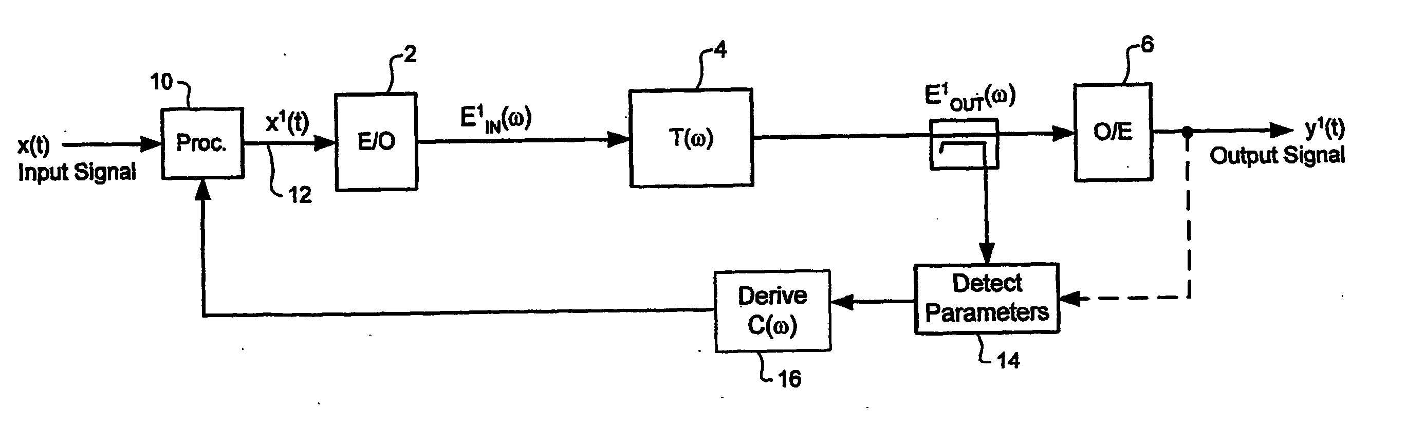
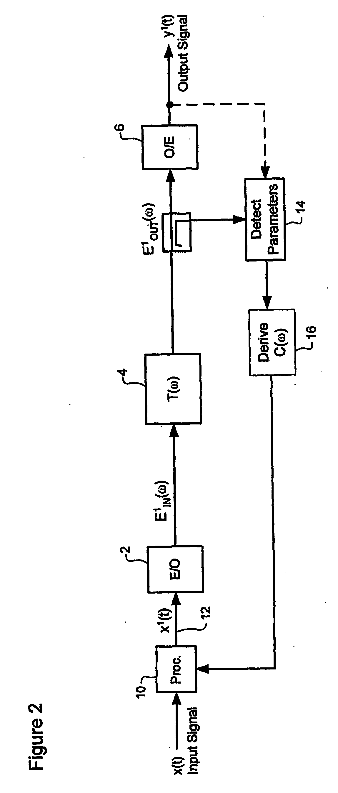
[0040] The present invention provides a method and system for compensation of chromatic dispersion in an optical communications system. FIG. 2 is a block diagram schematically illustrating principal operations in accordance with the method of the present invention.

[0041] As shown in FIG. 2, the optical communications system is represented by electrical-to-optical (E / O) and optical-to-electrical (O / E) converters 2 and 6 separated by an optical link 4 represented by a system transfer function T(ω). In accordance with the present invention, signal distortions introduced by the system transfer function T(ω) are compensated by deriving a compensation function C(ω) that optimizes system performance. A compensation processor 10 uses the compensation function C(ω) to filter the input signal x(t) in the electrical domain, thereby producing a predistorted input signal x1(t) 12 given by:

x1(t)=x(t) conv C(ω)

where “conv” is the convolution function.

[0042] The predistorted input signal x1(t)...


PUM


Abstract

Optical dispersion imposed on a communications signal conveyed through an optical communications system is compensated by modulating the communications signal in the electrical domain. A compensation function is determined that substantially mitigates the chromatic dispersion. The communications signal is then modulated in the electrical domain using the compensation function. In preferred embodiments, compensation is implemented in the transmitter, using a look-up-table and digital-to-analog converter to generate an electrical predistorted signal. The electrical predistorted signal is then used to modulate an optical source to generate a corresponding predistorted optical signal for transmission through the optical communications system.

Description

TECHNICAL FIELD [0001] The present invention relates to optical communications systems, and in particular to electrical domain compensation of optical dispersion in an optical communications system. BACKGROUND OF THE INVENTION [0002] Optical communications systems typically include a pair of network nodes connected by an optical waveguide (i.e., fiber) link. Within each network node, communications signals are converted into electrical signals for signal regeneration and / or routing, and converted into optical signals for transmission through an optical link to another node. The optical link between the network nodes is typically made up of multiple concatenated optical components, including one or more (and possibly 20 or more) optical fiber spans (e.g., of 40-150 km in length) interconnected by optical amplifiers. [0003] The use of concatenated optical components within a link enables improved signal reach (that is, the distance that an optical signal can be conveyed before being r...

Claims


Application Information

Patent Timeline
Patent Type & Authority Applications(United States)
IPC IPC(8): H04B10/12H04B10/155H04B10/18
CPCH04B10/25137H04B10/505H04B10/50597H04B10/508H04B10/07951H04B10/07953H04B10/6161
Inventor MCNICOL, JOHNPARSONS, KIERANSTRAWCZYNSKI, LEOROBERTS, KIMBO'SULLIVAN, MAURICES
Owner CIENA
Why Eureka
Try Eureka