Method for performing full-chip manufacturing reliability checking and correction

a technology of reliability checking and full-chip manufacturing, applied in the direction of photomechanical treatment originals, instruments, photomechanical equipment, etc., can solve the problems of substantial cost in both time and money associated with the redesign process, difficult and/or unsuitable use of known techniques in today's design layout, etc., to reduce time and cost, the effect of eliminating costs

Active Publication Date: 2006-04-13
ASML NETHERLANDS BV
View PDF28 Cites 19 Cited by
  • Summary
  • Abstract
  • Description
  • Claims
  • Application Information

AI Technical Summary

Benefits of technology

[0015] Yet another advantage of the present invention is that the full-chip manufacturing reliability checking and correction method is suitable for use with processes utilizing multiple masks and/or multiple exposures (e.g., DDL vertical and horizontal masks), and multiple data layers in the same mask (e.g., CPL masks including chrome and phase features).
[0016] Yet another advantage of the present invention is that the method provides feedback to the designer early in the design process regarding whether the target design contains any “trouble spots” or “weak spots” that would prevent the target design from satisfying the design requirements and/or result in an unsatisfactory yield when subjected to the manufacturing process. As a result, the present invention minimizes the time and costs associated with a redesign process, as well as eliminates the costs associated with tape-out and development of a prototype of a flawed design. In other words, the present invention allows the designer to determine whether or not a design is fundamentally flawed (and therefore non-manufacturable) before the tape-out process and development (i.e., processing) of a test wafer.
[0017] In addition, the method of the

Problems solved by technology

These rules are set by processing and design limitations.
While various rule checking methods have been discussed in the prior art, such as optical rule checking (ORC), these known techniques are difficult and/or unsuitable for use with today's design layouts, which typically include advanced resolution enhancem

Method used


Image

  • Method for performing full-chip manufacturing reliability checking and correction
  • Method for performing full-chip manufacturing reliability checking and correction
  • Method for performing full-chip manufacturing reliability checking and correction

Examples


Embodiment Construction

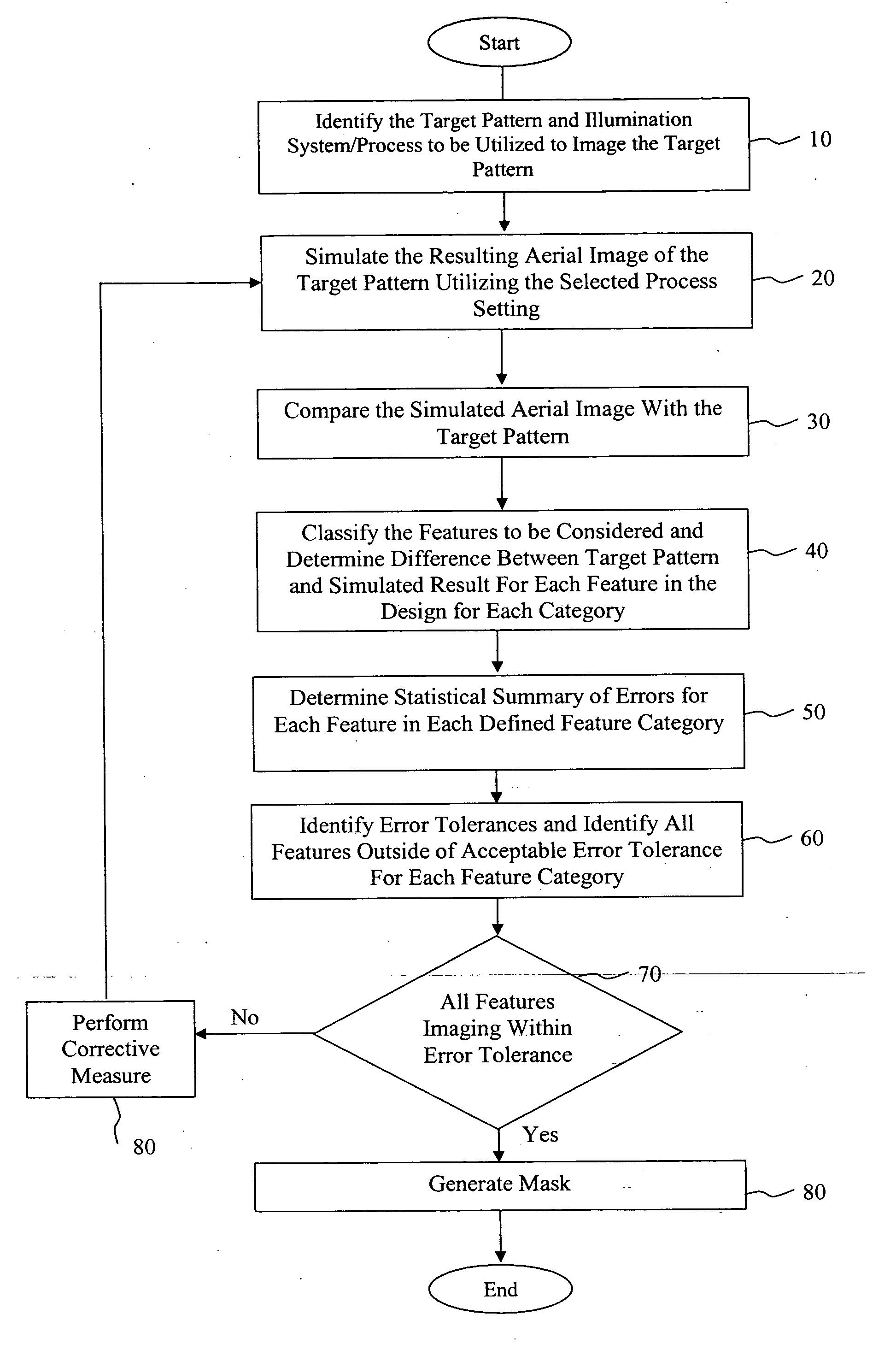
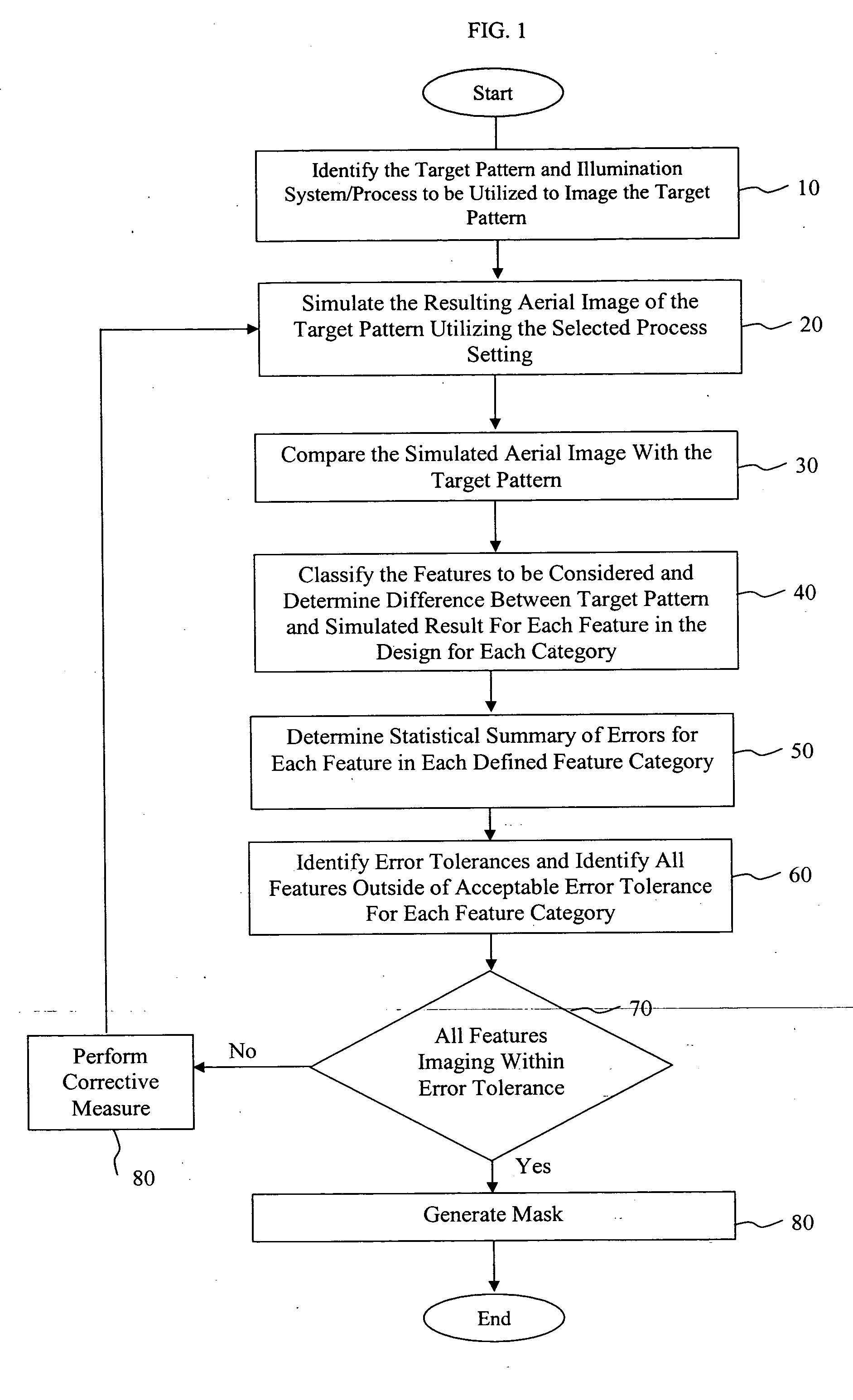
[0030]FIG. 1 is an exemplary flowchart illustrating the full-chip manufacturing reliability checking and correction method in accordance with a first embodiment of the present invention. The first step (Step 10) in the process is to identify the target mask pattern (i.e., the target design) and illumination system and settings (i.e., process conditions) to be utilized to image the pattern.

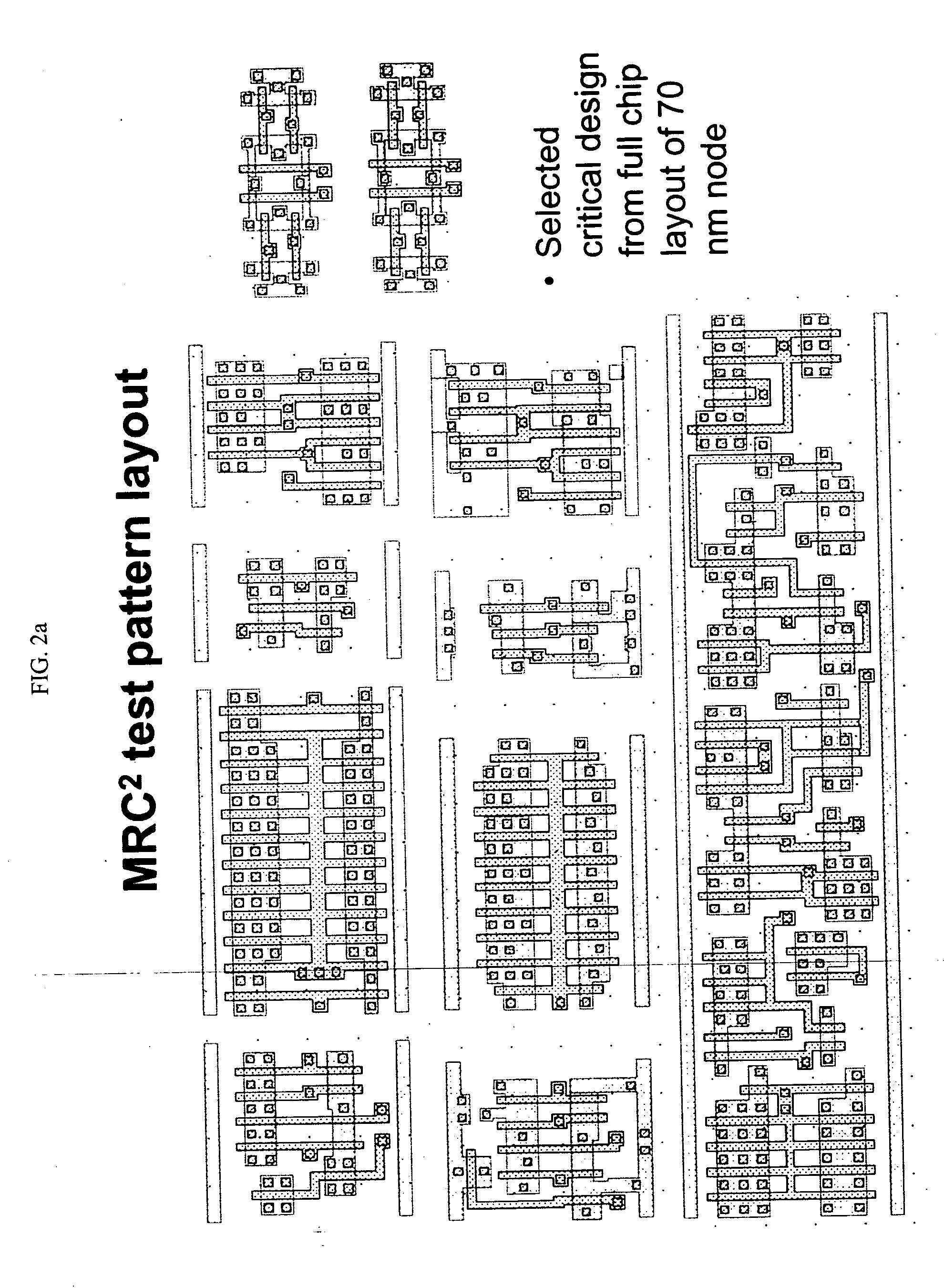
[0031]FIGS. 2a and 2b illustrate an exemplary layout pattern (i.e., target pattern) that can be subjected to the checking and correction method of the present invention. More specifically, FIG. 2a represents the full chip layout, while FIG. 2b represents a portion of the layout of FIG. 2a separated into chrome and phase areas in a CPL mask. As noted above, the method of the present invention is suitable for use with processes utilizing multiple masks and / or multiple exposures (e.g., DDL vertical and horizontal masks), and multiple data layers in the same mask (e.g., CPL masks including chrome and ...


PUM


Abstract

A method of generating a mask for use in an imaging process pattern. The method includes the steps of: (a) obtaining a desired target pattern having a plurality of features to be imaged on a substrate; (b) simulating a wafer image utilizing the target pattern and process parameters associated with a defined process; (c) defining at least one feature category; (d) identifying features in the target pattern that correspond to the at least one feature category, and recording an error value for each feature identified as corresponding to the at least one feature category; and (e) generating a statistical summary which indicates the error value for each feature identified as corresponding to the at least one feature category.

Description

CLAIM OF PRIORITY [0001] This patent application, and any patent(s) issuing therefrom, claims priority to U.S. provisional patent application No. 60 / 609,243, filed on Sep. 14, 2004, entitled “Full-Chip Manufacturing Reliability Check And Correction (MRC2)”, which is incorporated herein by reference in its entirety.TECHNICAL FIELD [0002] The technical field of the present invention relates generally to a method, program product and apparatus for allowing for the determination earlier on in the design process of whether the target design / layout is manufacturable utilizing a given process, or whether the target design / layout contains “trouble spots” or “weak spots,” that would prevent the target design / layout from satisfying the design requirements and / or result in an unsatisfactory yield when manufactured. BACKGROUND OF THE INVENTION [0003] Lithographic apparatus can be used, for example, in the manufacture of integrated circuits (ICs). In such a case, the mask may contain a circuit p...

Claims


Application Information

Patent Timeline
IPC IPC(8): G06F17/50G03F1/00G03F1/36
CPCG03F1/36G03F7/70433G03F7/70441G03F7/705
Inventor HSU, MICHAELLAIDIG, THOMASWAMPLER, KURTHSU, DUAN-FUSHI, XUELONG
Owner ASML NETHERLANDS BV
Why Eureka
Try Eureka