

Semiconductor device, manufacturing method thereof, and memory circuit
a technology of semiconductor devices and memory circuits, applied in semiconductor devices, electrical devices, transistors, etc., can solve problems such as the decrease of the resistance of source-drain voltage, and achieve the effect of stabilizing operation
- Summary
- Abstract
- Description
- Claims
- Application Information
AI Technical Summary
Benefits of technology
Problems solved by technology
Method used
Image

Examples
first embodiment
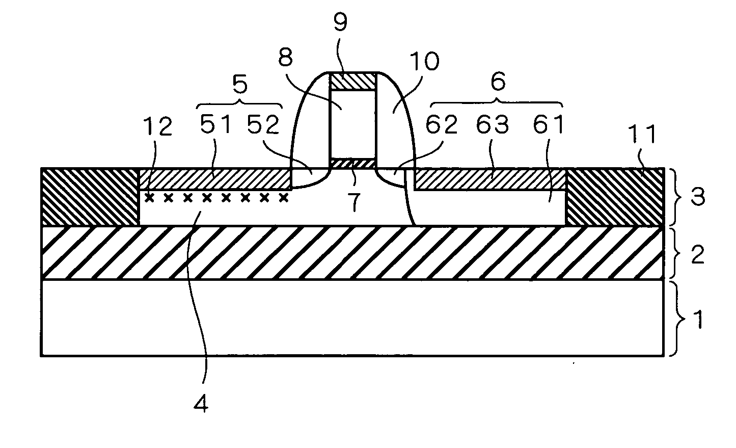
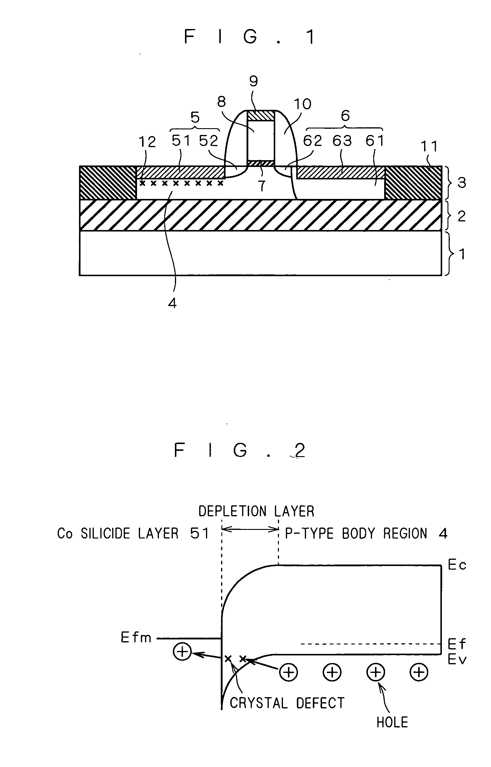
[0038]FIG. 1 is a sectional view of a semiconductor device according to a first embodiment. The semiconductor device shown in FIG. 1 has an SOI structure, in which a buried oxide film 2 is formed on a silicon substrate 1 and, further, a semiconductor layer 3 is formed on the buried oxide film 2. Since an N channel-type MOS transistor is formed in the semiconductor layer 3, a P-type body region 4, an N-type source region 5 and an N-type drain region 6 are provided.
[0039] The source region 5 includes a Co silicide layer 51 which makes contact with the body region 4 at its bottom face, and an N-type source extension layer 52 which makes contact with a side face of the Co silicide layer 51. The drain region 6 includes an N-type drain diffusion region 61 which makes contact with the buried oxide film 2, an N-type drain extension layer 62 which makes contact with a side face of the drain diffusion layer 61, and a Co silicide layer 63 which is formed so as to be buried into the N-type dra...
second embodiment
[0053] In a semiconductor device having an SOI structure, a body floating effect can be suppressed also by decreasing generation of hot carriers. In order to decrease the generation of such hot carriers, it is enough to lessen an electric field in a drain region at a gate electrode side. That is, a source region is made in a source impurity structure which is low in parasitic resistance, and an asymmetrical source-drain structure is formed, so that the electric field in the drain region at the gate electrode side can be lessened. This structure is employed in a semiconductor device according to a second embodiment.
[0054] Specifically, the semiconductor device according to this embodiment is described. The structure of the semiconductor device according to this embodiment is basically same as the structure shown in FIG. 1. This embodiment is, however, different from the first embodiment in that the impurity concentration of the source extension layer 52 is different from impurity co...
third embodiment
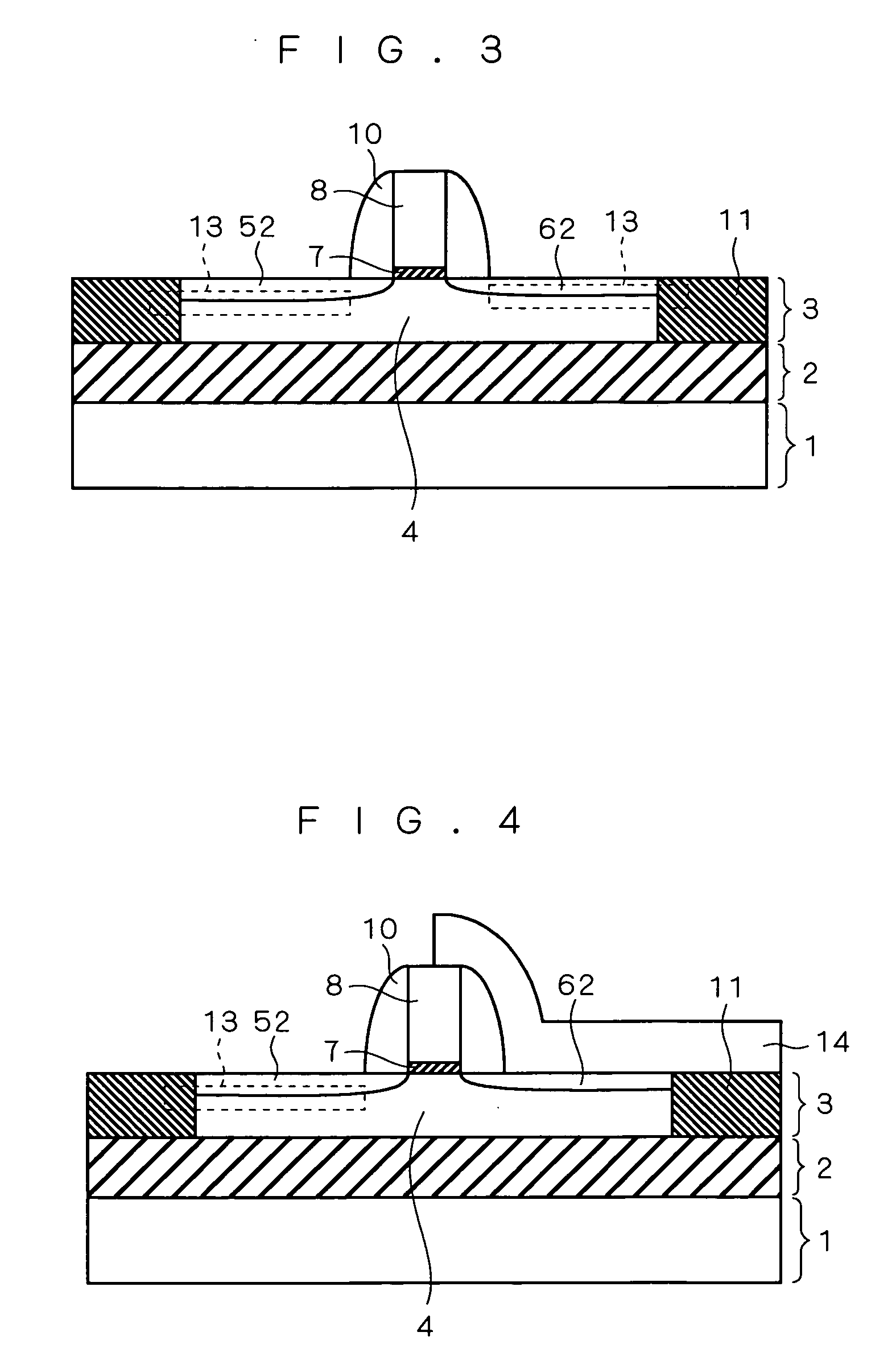
[0059]FIG. 7 is a sectional view of a semiconductor device according to a third embodiment. The semiconductor device in FIG. 7 differs from the structure of the source region 5 shown in FIG. 1. All other parts than the source region 5 in FIG. 7 are same as in the semiconductor device shown in FIG. 1, and same parts are denoted by the same reference numerals and detailed description will not be given herein.
[0060] The source region 5 shown in FIG. 7 includes a source extension layer 52 formed in the vicinity of a gate oxide film 7, a Co silicide layer 51 formed in a side direction of a source extension layer 52, an N-type source diffusion layer 53 formed under the Co silicide layer 51, and a P-type diffusion layer 54 formed under the source diffusion layer 53. The P-type diffusion layer 54 makes contact with the source diffusion layer 53 in a wider area as compared with the contact area of the source diffusion layer 53 and a body region 4. The P-type diffusion layer 54 is higher in ...
PUM
 Abstract
Description
Claims
Application Information