Semiconductor package

Inactive Publication Date: 2006-04-20
HIMAX TECH LTD
View PDF5 Cites 22 Cited by
  • Summary
  • Abstract
  • Description
  • Claims
  • Application Information

AI Technical Summary

Benefits of technology

[0013] According to another feature of the present invention, the semiconductor package comprises two conductive supporting lines respectively disposed on two opposite sides of the substrate thereby enhancing the mechanical strength of the substrate, and a plurality of sprocket holes provided on the two conductive supporting lines. The plurality of substrate units are substantially arranged in a r

Problems solved by technology

Therefore, the TAB packaging technology will be limited in application; more specifically, the I/O leads pitch of the TAB package is not easy to meet the requirement of the higher-resolution displays.
Besides, the inner leads of the TAB package stay floated and are not supported by a polyimide (PI) film; therefore, they are weak in mechanical strength and thus easy to become deformed.
However, the above-mentioned LCD driver IC packages have one disadvantage; that is,

Method used


Image

  • Semiconductor package
  • Semiconductor package
  • Semiconductor package

Examples


Embodiment Construction

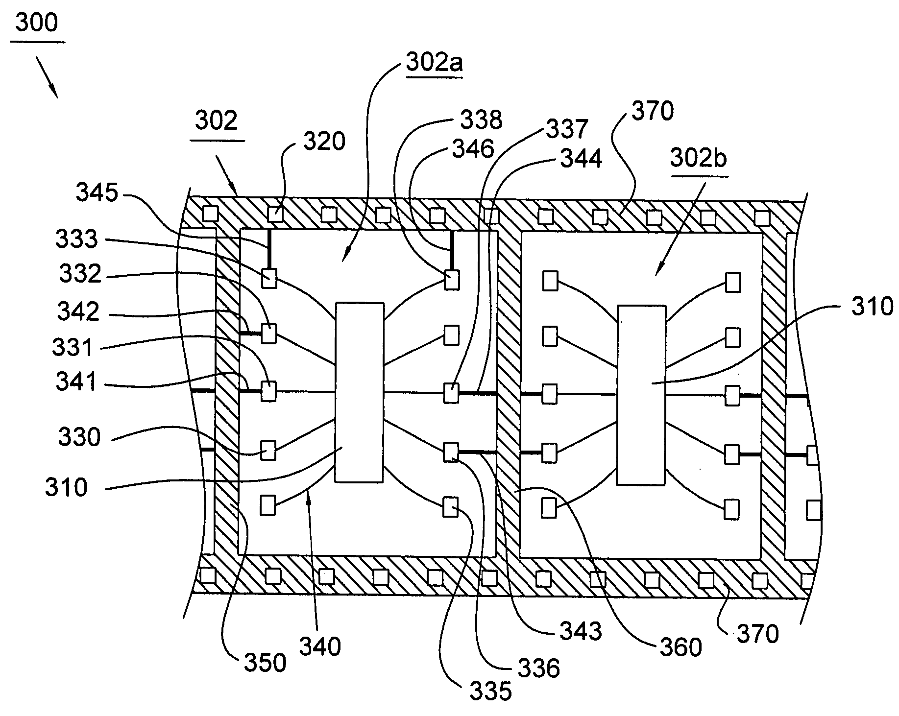
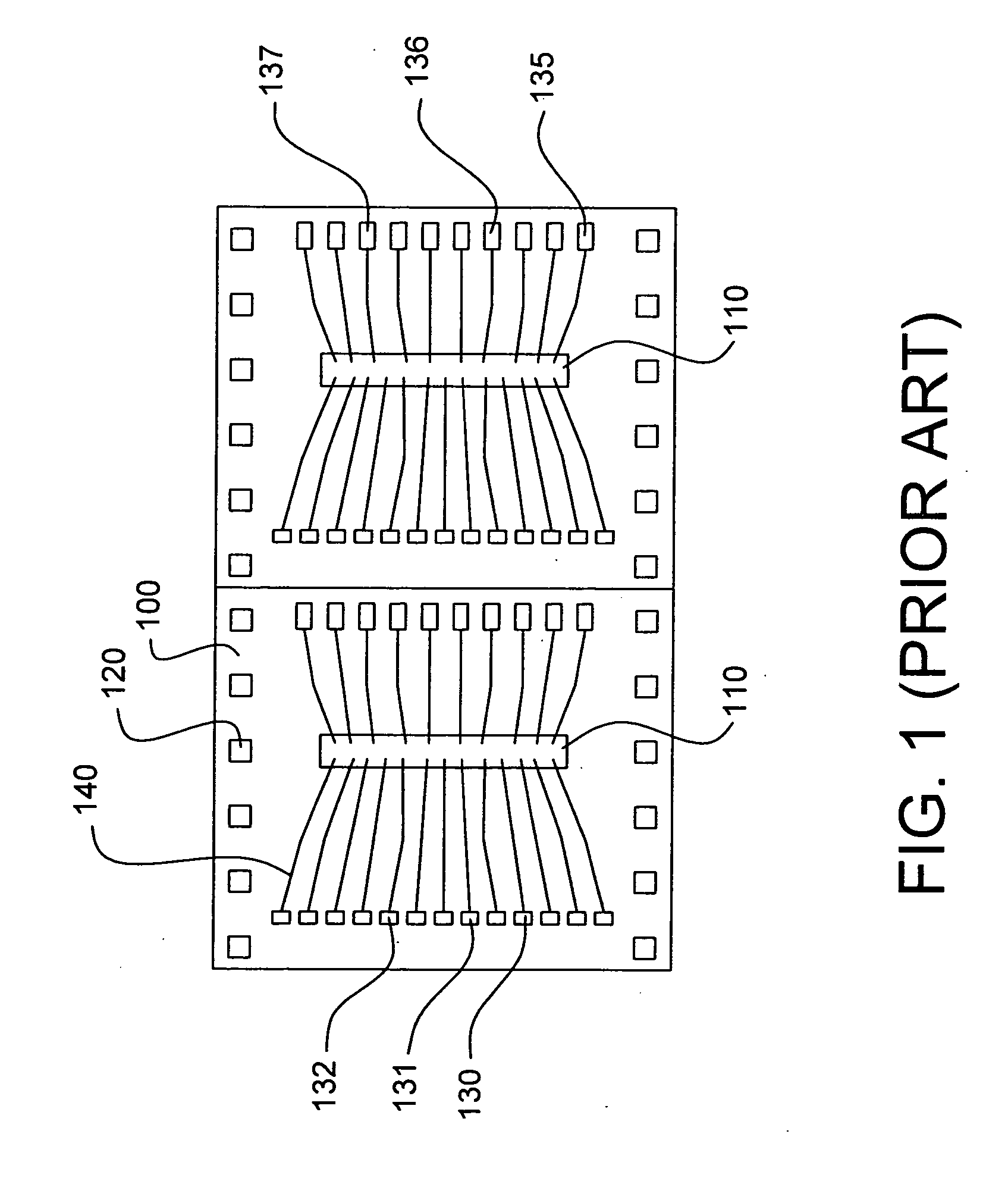
[0019] In order to better understand the features of the present invention, it is needed to illustrate the conventional LCD driver IC package. Referring to FIG. 1, a conventional LCD driver IC package mainly comprises a substrate 100, a semiconductor chip 110, a plurality of sprocket holes 120, and a plurality of contact pads 130, 131, 132, 135, 136 and 137. The substrate 100 has an upper surface and a lower surface, and is provided with the contact pads 130, 131, 132, 135, 136 and 137. These contact pads include signal pads, ground pads and dummy pads. For example, the contact pad 130 can be signal pad, the contact pad 131 can be ground pad, and the contact pad 132 can be dummy pad. The semiconductor chip 110 is disposed on the upper surface of the substrate 100 and electrically connected to the contact pads through conductive leads 140. The plurality of sprocket holes 120 are used for cooperating with the sprocket gear of a transporter (not shown) such that the IC package can be t...


PUM


Abstract

The present invention discloses a semiconductor package comprising a substrate having a plurality of substrate units, a plurality of semiconductor chips respectively disposed on the substrate units, and a plurality of conductive guard lines each disposed between two adjacent substrate units. Each substrate unit is provided with a plurality of contact pads and a plurality of conductive leads respectively connected to the corresponding contact pads. The semiconductor chips are electrically connected to the plurality of contact pads through the conductive leads. Each substrate unit has at least one of the contact pads electrically connected to the conductive guard lines such that the semiconductor package of the present invention can efficiently achieve the function of electrostatic discharge (ESD) protection.

Description

BACKGROUND OF THE INVENTION [0001] 1. Field of the Invention [0002] This invention generally relates to a semiconductor package, and more particularly to a semiconductor package for liquid crystal display driver, which can efficiently achieve the function of electrostatic discharge (ESD) protection. [0003] 2. Description of the Related Art [0004] In the prior art, liquid crystal display (LCD) or plasma display panels have been widely applied to many electronic products. Generally, either of these display panels has the outer leads of its display driver packages attached to the pads (or leads) disposed on the boundary portion of a lower glass substrate. [0005] With the increasing requirements for more complicated electronic apparatuses, the speed and complexity of semiconductor chips have become relatively higher and higher. Accordingly, higher packaging efficiency for the semiconductor chips is required nowadays. The current packaging technology for driver ICs of the LCD panel inclu...

Claims


Application Information

Patent Timeline
IPC IPC(8): H01L23/02
CPCH01L23/49838H01L23/62H01L2224/16H01L2924/01079
Inventor BAI, SHWANG SHICHANG, JUNG CHUNGCHENG, PAI SHENGWU, CHIA HUI
Owner HIMAX TECH LTD
Why Eureka
Try Eureka