Method for circuit sensitivity driven parasitic extraction

Active Publication Date: 2006-04-20
TEXAS INSTR INC
View PDF7 Cites 0 Cited by
  • Summary
  • Abstract
  • Description
  • Claims
  • Application Information

AI Technical Summary

Benefits of technology

[0007] This invention ensures accuracy for all types of applications, such as hold-time and setup-time in digital circuits. It is also app

Problems solved by technology

One of the most difficult tasks in integrated circuit design is timing closure.
However, the wire capacitance generally includes a considerable proportion of parasitic capacitance.
Parasitic capacitance varies widely and can be particularly difficult to estimate in current designs with multi-level metal and large numbers of crowded

Method used


Image

  • Method for circuit sensitivity driven parasitic extraction
  • Method for circuit sensitivity driven parasitic extraction
  • Method for circuit sensitivity driven parasitic extraction

Examples


Example

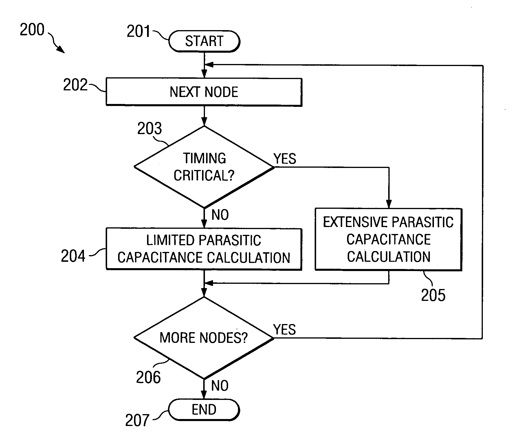
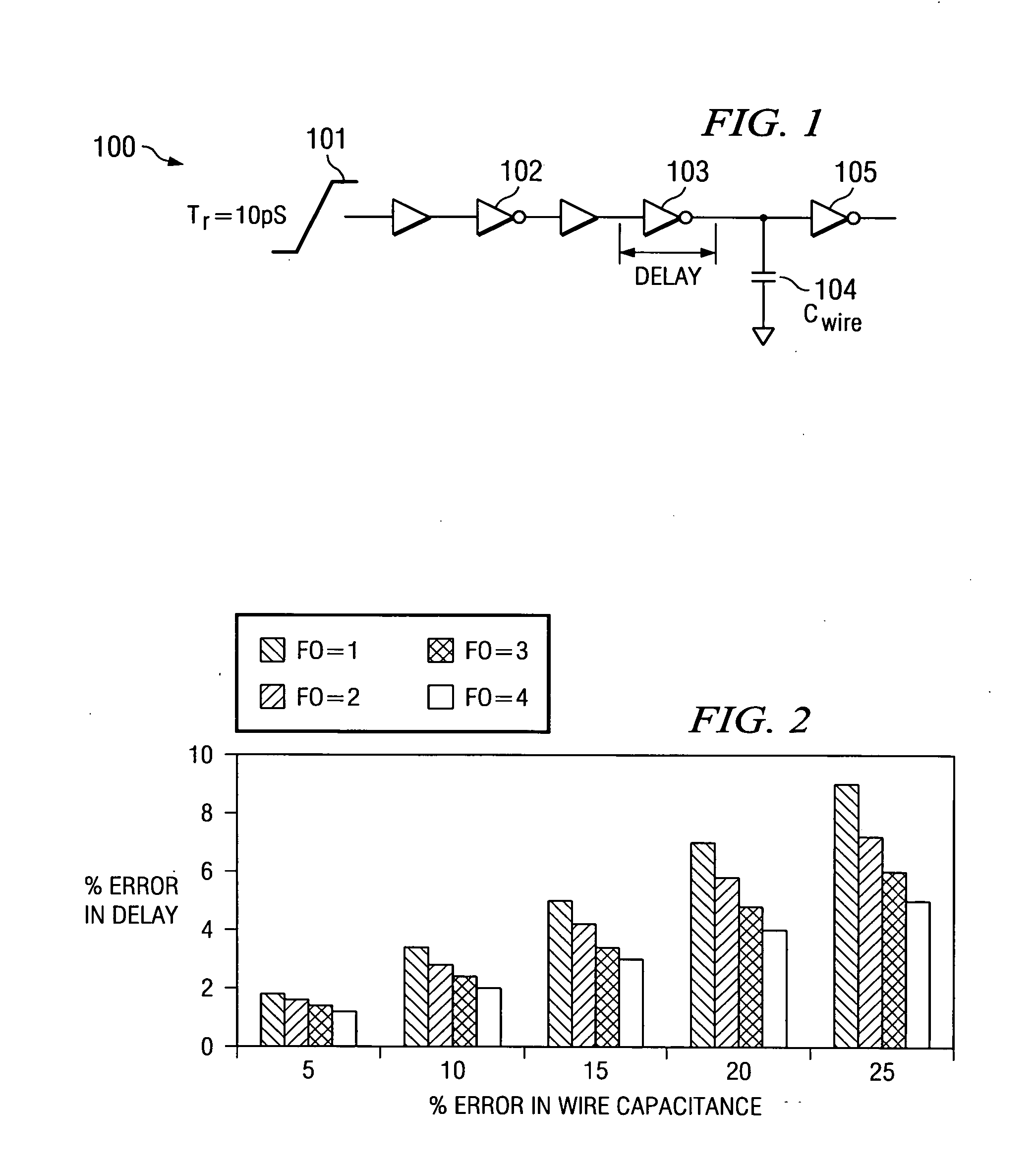
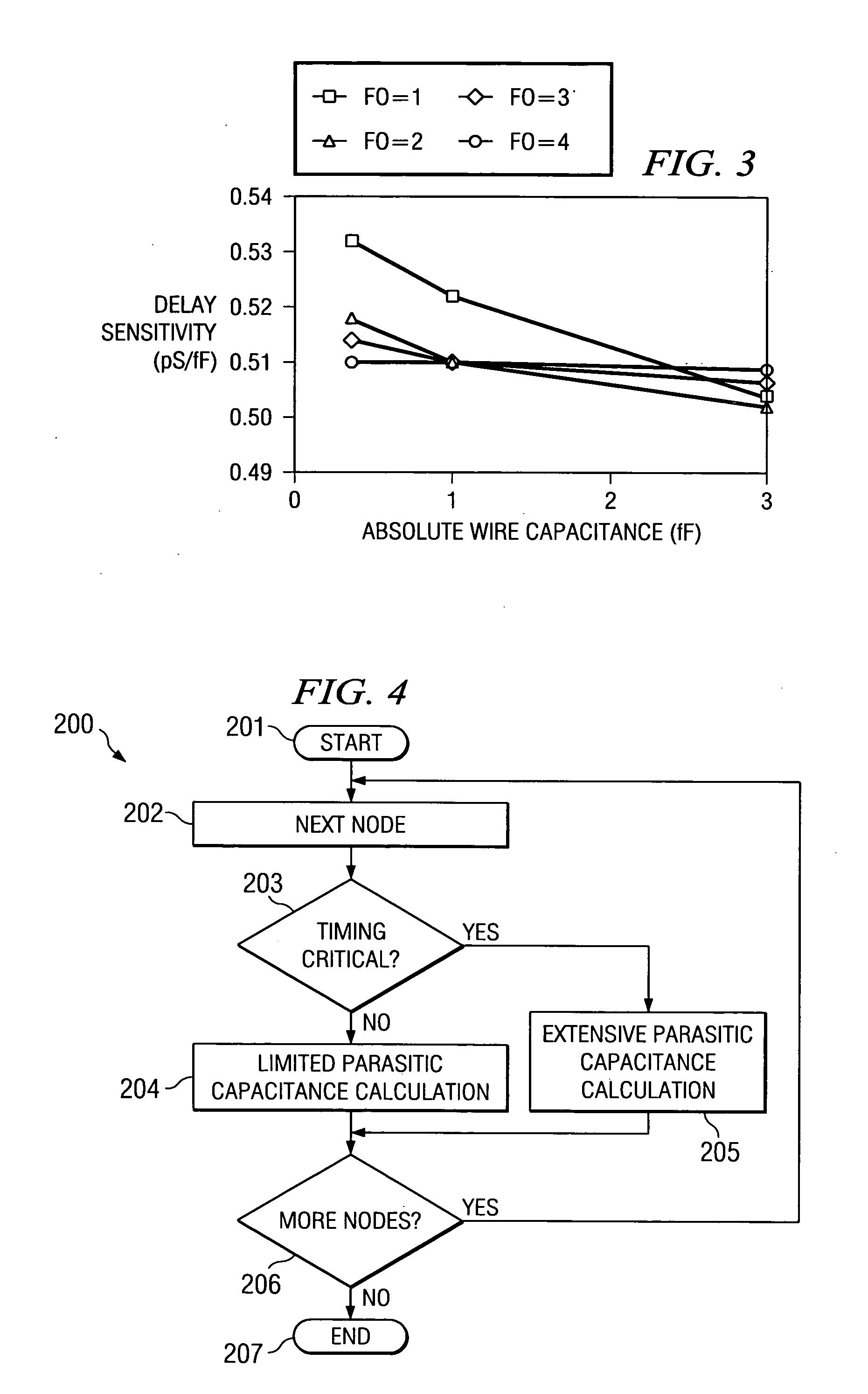
[0013] Historically most parasitic capacitance extraction tools use a capacitance accuracy metric. Thus the tool could operate to ensure accuracy within ±5% of the actual silicon capacitance or a reference extraction, such as Quickcap 3-D field solver. Thus most parasitic capacitance extraction tools find it difficult to meet a reasonable accuracy versus runtime trade-off. Due to 3-D effects and process complexities such as Selective Process Bias (SPB) and dummy metal geometries, high accuracy parasitic capacitance calculation is time consuming.

[0014] Critical performance metrics for the integrated circuit design are delay and noise. These are a combined effect of circuit configuration and RC parasitics. Not all network nodes in a particular integrated circuit design need high accuracy extraction. Thus runtimes can be lowered by employing a variable accuracy extraction. Some critical network nodes will require highly accurate parasitic capacitance extraction to yield information ne...


PUM


Abstract

The method of this invention determines the timing of an integrated circuit design. At each node, the method determines if the timing of signal propagation at that node is critical. If this timing is critical, method calculates the capacitance at said current node using a highly accurate but computationally intensive model. If this timing is not critical, the method uses a less accurate but less computationally intensive model. The method calculates a signal delay for each mode from the drive strength, calculated capacitance and fan-out. This signal delay is compared to a design goal. This method achieves a better trade-off between timing determination run-time and accuracy. Timing criticality can be determined from one or more of conductor length/area, fan-out, logic depth and timing slack.

Description

CLAIM OF PRIORITY [0001] This application claims priority under 35 U.S.C. 119(e)(1) from U.S. Provisional Application 60 / 619,845 filed Oct. 18, 2004.TECHNICAL FIELD OF THE INVENTION [0002] The technical field of this invention is microelectronic design tools and especially the use of parasitic capacitance extraction. BACKGROUND OF THE INVENTION [0003] The design very high speed and high precision integrated circuits involves many design choices and trade-offs. One of the most difficult tasks in integrated circuit design is timing closure. Achieving timing closure means that all the parts of the integrated circuit generate their outputs in time for proper operation of the next circuit. The rise time on a signal line varies directly with the drive capacity of the driving circuit. The drive capacity typically varies directly with the channel width of the driving transistors. This rise time varies inversely with the capacitance driven. The driven capacitance includes the gate capacitanc...

Claims


Application Information

Patent Timeline
IPC IPC(8): G06F9/45G06F17/50
CPCG06F17/5022G06F30/33
Inventor NARASIMHA, USHAHILL, ANTHONY M.SAVITHRI, NAGARAJ NARASIMH
Owner TEXAS INSTR INC
Why Eureka
Try Eureka