Semiconductor device

a technology of semiconductor devices and semiconductors, applied in semiconductor devices, semiconductor/solid-state device details, electrical apparatus, etc., can solve the problems of difficult to inhibit the percolation of water, a metal ion, and an organic matter from a portion of the fuse b, and achieve excellent reliability, prevent degradation of circuit elements functionality, excellent reliability

Active Publication Date: 2006-04-27
RENESAS ELECTRONICS CORP
View PDF11 Cites 8 Cited by
  • Summary
  • Abstract
  • Description
  • Claims
  • Application Information

AI Technical Summary

Benefits of technology

[0015] By this configuration, a potential of a positively charged p-type well can thrust back positively charged water, metal ions, and organic matters that may percolate from a portion where the fuse is removed after the fuse trimming. It is thus possible to inhibit the water, metal ions, or organic matters that have percolated from a damaged portion of an insulating layer from percolating to an outside of the p-type well when melting the fuse by laser irradiation. Accordingly, by arranging circuit elements outside the p-type well, it is possible to prevent degradation in functionality of the circuit elements. By this configuration, therefore, a semiconductor device having an excellent reliability can be obtained.
[0016] The present invention provides a semiconductor device that has an excellent reliability because it has a special well structure below a fuse.

Problems solved by technology

However, although by the conventional technologies described in the above Japanese Laid-open patent publication No. 10-223762 it is possible to inhibit percolation of, for example, water from a portion between the first interconnection 16 and the second interconnection 22 and from the cover opening 25 outside the metal sidewall portion 21a, it is difficult by these technologies to inhibit percolation of water, a metal ion, and an organic matter from a portion of the fuse 12 damaged by fuse trimming.

Method used


Image

  • Semiconductor device
  • Semiconductor device
  • Semiconductor device

Examples


first embodiment

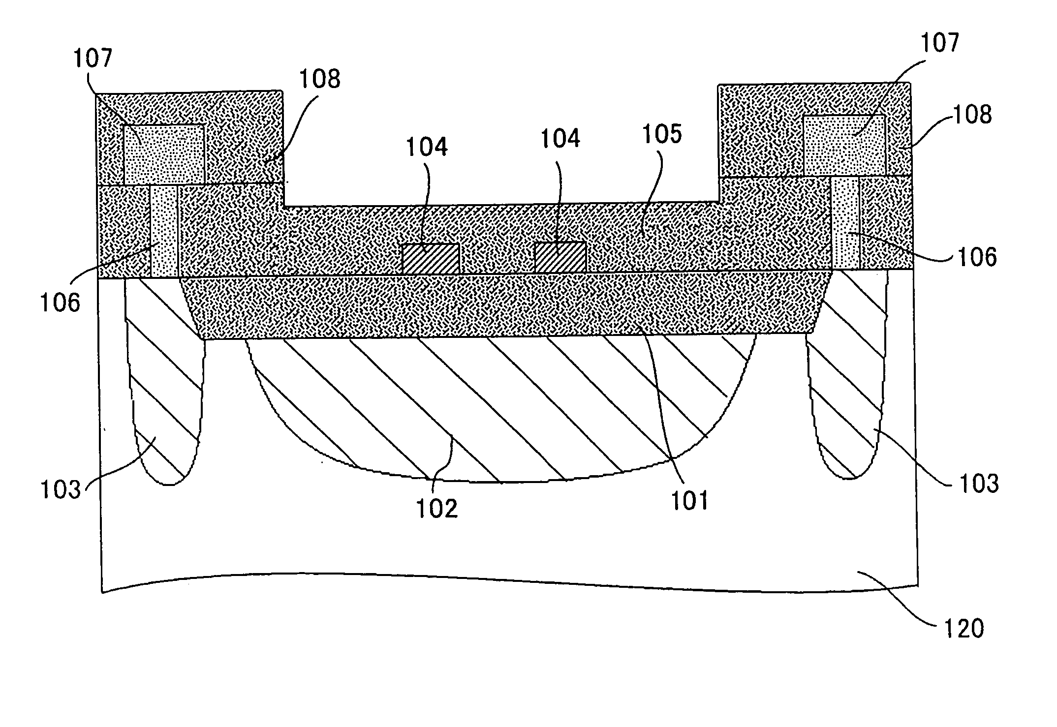
[0035]FIG. 1 is a cross-sectional view of a configuration of a laser-trimming fuse used in the present embodiment.

[0036] A semiconductor device according to the present embodiment comprises a p-type silicon substrate 120 (semiconductor substrate). On the silicon substrate 120, a field oxide film 101 (insulating layer) is provided. The field oxide film 101 is an element separation film (STI) made of an SiO2 film embedded on the element formation surface side of the silicon substrate 120. On the field oxide film 101, two fuses 104 are provided.

[0037] In the silicon substrate 120, an n-type well 102 is provided directly below the fuses 104. The n-type well 102 is configured so as to come into contact with a lower surface of the field oxide film 101. A p-type well 103 is provided in such a manner as to surround a region directly below the fuses 104 in the silicon substrate 120.

[0038] An impurity concentration of the p-type well 103 is larger than that of the other p-type regions in t...

second embodiment

[0061] A configuration of a semiconductor device according to the present embodiment is basically the same as that of the semiconductor according to the first embodiment, except that the semiconductor device according to the present embodiment employs a seal ring composed of a two-step contact and a two-step interconnection as described later.

[0062] The following will describe steps of manufacturing the semiconductor device according to the present embodiment.

[0063]FIGS. 3A to 3C are process cross-sectional view showing a method of manufacturing the semiconductor device according to the present embodiment in order of its manufacturing steps. First, as shown in FIG. 3A, on a silicon substrate 220, a field oxide film 201 is formed in a fuse element portion in order to electrically insulate device elements from each other.

[0064] This field oxide film 201 can be formed by the same process as that of the other field oxide films that define a circuit element region.

[0065] Next, as sho...


PUM


Abstract

On a silicon substrate 120 of a semiconductor device, a field oxide film 101 is provided. On the field oxide film 101, two fuses 104 are provided. Directly below the fuses 104 in the silicon substrate 120, an n-type well 102 is provided. Besides the n-type well 102, a p-type well 103 is provided in such a manner as to surround a region directly under the fuses 104 in the silicon substrate 120. A cover insulating film 108 is provided over the silicon substrate 120 and the field oxide film 101. A seal ring composed of a contact 106 and an interconnection 107 is embedded in the cover insulating film 108 so as to surround the fuses 104.

Description

[0001] This application is based on Japanese Patent application NOs. 2004-311284 and 2005-287792, the contents of which are incorporated hereinto by reference. FIELD OF THE INVENTION [0002] The present invention relates to a semiconductor device. DESCRIPTION OF THE RELATED ART [0003] Recently, semiconductor circuits have began to be used in products such as an automobile that are required to be highly reliable, so that reliable technologies have also began to be required for manufacturing each of factor components of these circuits such as a transistor and an interconnection. A semiconductor is generally manufactured by forming a large number of circuit elements such as a transistor, a resistor, and a capacitor on a semiconductor substrate and interconnecting these elements so as to satisfy required circuit operations and functions. So-called fuses are used in a factor technology for a semiconductor circuit, to cut off a memory circuit on which a fault is found or a redundant circui...

Claims


Application Information

Patent Timeline
Patent Type & Authority Applications(United States)
IPC IPC(8): H01L29/00
CPCH01L23/5258H01L23/564H01L2924/0002H01L2924/00H01L21/82
Inventor MIWA, KIYOTAKAKARIYA, NAYUTA
Owner RENESAS ELECTRONICS CORP
Why Eureka
Try Eureka