Analog storage cell with low leakage

a technology of analog storage cell and low leakage, applied in the direction of electrical analogue stores, pulse techniques, instruments, etc., can solve the problems of high voltage required for writing to the cell, disadvantages of added circuit complexity and power, and the technique does not focus on characterizing the leakage of switches, etc., to achieve the effect of reducing the conduction of accumulation mod

Active Publication Date: 2006-04-27
MASSACHUSETTS INST OF TECH
View PDF12 Cites 10 Cited by
  • Summary
  • Abstract
  • Description
  • Claims
  • Application Information

AI Technical Summary

Benefits of technology

[0010] In a further aspect of the invention, a method includes coupling, to form an analog storage cell circuit, a switch to a sample and hold circuit, the switch including a first switching device forming a core of the switch, a second switching device coupled to the first switching device to disconnect the first switching device from a first terminal during the hold phase, and a third switching device coupled to the first switching device to connect the first switching device to a second terminal during the hold phase to minimize accumulation mode conduction in the first switching device.

Problems solved by technology

This form of storage is a very compact, low-power, and precise storage technique, but is useful only for relatively short time scales since the OFF state leakage of the MOS switch quickly degrades the stored charge.
However, these techniques do not focus on characterizing the switch leakage as a function of terminal voltages.
This scheme has the disadvantages of added circuit complexity and power due to both the analog-to-digital converter and the bussing required for multiplexing the converter between cells.
Disadvantages of this scheme include high voltages required for writing to the cells, slow write times, and additional supporting circuitry and bussing to accomplish the writing.

Method used


Image

  • Analog storage cell with low leakage
  • Analog storage cell with low leakage
  • Analog storage cell with low leakage

Examples


Embodiment Construction

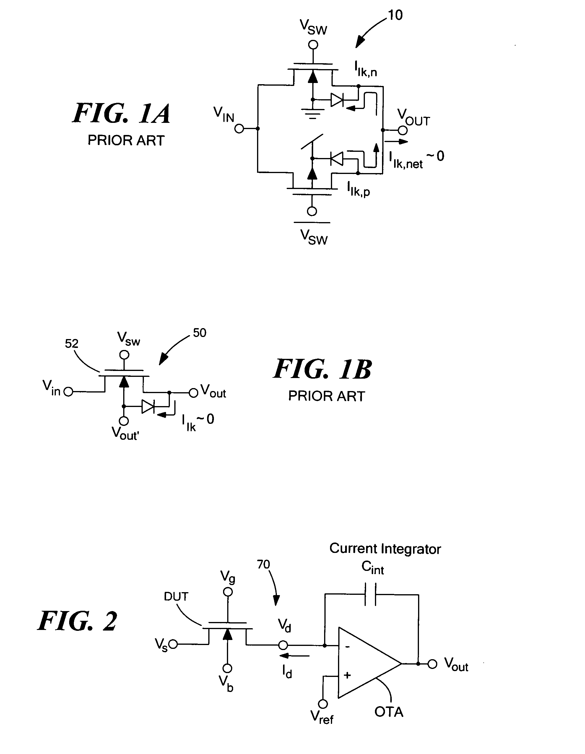
[0032] Before describing the invention in detail, some introductory information is presented. Medium-term analog storage cells achieve extended hold times by reducing the MOS-switch leakage current that degrades the cell's capacitively held charge. The lowest-leakage storage cell implementations have employed several different techniques to reduce switch leakage. These techniques are briefly reviewed below, and then a unified framework for comparing the performance of past implementations, which were fabricated in various technologies, is introduced.

[0033]FIGS. 1A and 1B show known low-leakage MOS switches used in analog storage cells. FIG. 1A shows a transmission gate switch 10 and two leakage currents, Ilk,n and Ilk,p, that can flow to Vout even when the switch is off. Leakage current Ilk,n flows from Vout to ground through the NMOS drain-to-bulk diode and Ilk,p flows from VDD to Vout through the PMOS drain-to-bulk diode. Since only the difference between these two leakage curren...


PUM


Abstract

An analog storage cell circuit includes a switch that minimizes subthreshold conduction and diode leakage, as well as an accumulation-mode coupling mechanism to minimize overall switch leakage to minimize accumulation-mode leakage. In one embodiment, an analog storage circuit includes a sample and hold circuit including an amplifier having first and second inputs and a switch coupled to the first input of the amplifier. The switch includes a first switching device forming a core of the switch, a second switching device coupled to the first switching device to disconnect the first switching device from a first terminal during the hold phase, and a third switching device coupled to the first switching device to connect the first switching device to a second terminal during the hold phase to minimize accumulation mode conduction in the first switching device.

Description

CROSS REFERENCE TO RELATED APPLICATIONS [0001] The present application claims the benefit of U.S. Provisional Patent Application No. 60 / 620,911, filed on Oct. 21, 2004, which is incorporated herein by reference.STATEMENT REGARDING FEDERALLY SPONSORED RESEARCH [0002] The Government may have certain rights in the invention pursuant to Contract No. NSF CCR-0122419 with the NSF and N00014-02-0434 with the ONR.BACKGROUND OF THE INVENTION [0003] As is known in the art, many modem analog CMOS (Complementary Metal-Oxide Semiconductor) circuits employ temporary analog storage to counteract circuit offsets and store signal variables and implement adaptation and learning. Offset correction and signal storage are common applications of temporary analog storage due to their widespread use in switched capacitor circuits, and straightforward implementation is possible using only a capacitor and a MOS switch. This form of storage is a very compact, low-power, and precise storage technique, but is u...

Claims


Application Information

Patent Timeline
Patent Type & Authority Applications(United States)
IPC IPC(8): H03K17/687
CPCG11C27/02G11C27/024H03K17/162
Inventor O'HALLORAN, MICAH GALLETTASARPESHKAR, RAHUL
Owner MASSACHUSETTS INST OF TECH
Why Eureka
Try Eureka