
Method of forming SRAM cell

a memory cell and sram technology, applied in the field of memory cell formation, can solve the problems of reducing the characteristics of the vcc margin of the power supply voltage, and the static noise margin is not improved, and achieve the effect of reducing the threshold voltage mismatch

Inactive Publication Date: 2006-04-27
SAMSUNG ELECTRONICS CO LTD
View PDF8 Cites 4 Cited by
  • Summary
  • Abstract
  • Description
  • Claims
  • Application Information

AI Technical Summary

Benefits of technology

[0008] The present invention provides a method of forming a static random access memory (SRAM) cell for reducing threshold voltage mismatch between transistors connected to two nodes of a bit line and a bit line bar.

Problems solved by technology

Unless the threshold voltage mismatch can be reduced to the minimum, power supply voltage Vcc margin characteristics are reduced due to the decrease of a cell current, and the static noise margin is not improved.

Method used


Image

  • Method of forming SRAM cell
  • Method of forming SRAM cell
  • Method of forming SRAM cell

Examples


Embodiment Construction

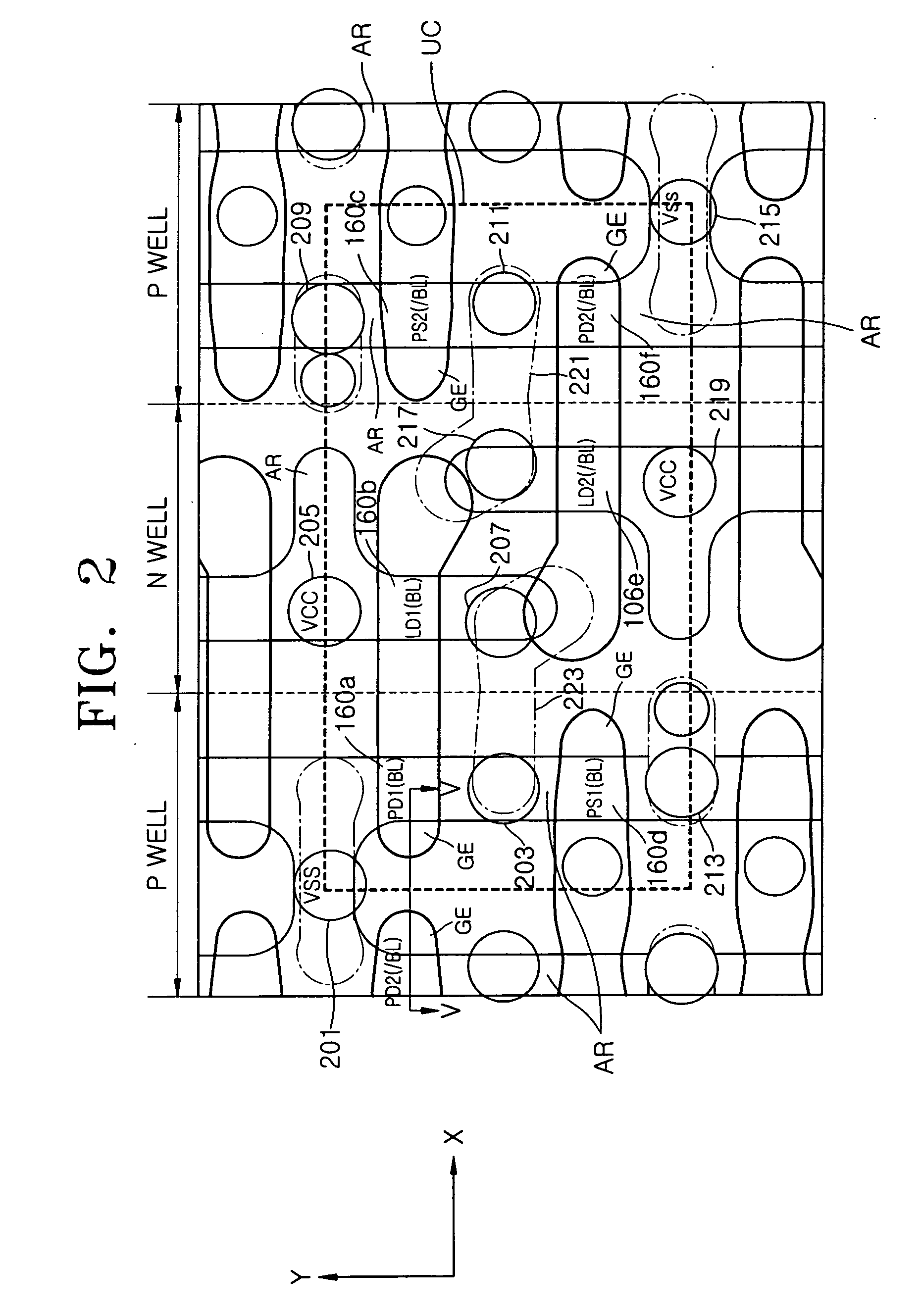
[0025] The present invention described herein can be applied to a static random access memory (SRAM) cell using a high load resistor cell or a CMOS type cell, but the present invention will be described in connection with an example of the CMOS type SRAM cell.

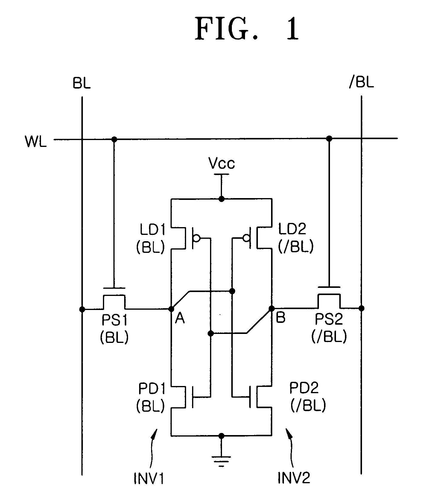
[0026]FIG. 1 is an equivalent circuit diagram illustrating one example of the CMOS type SRAM cell according to the present invention.

[0027] In particular, the CMOS type SRAM cell is disposed at the cross-section part of a pair of complementary bit lines, that is, a bit line BL and a bit line bar / BL, and a word line WL. The CMOS type SRAM cell is composed of a pair of driver transistors PD1, PD2, a pair of transfer transistors PS1, PS2, and a pair of load transistors LD1, LD2. The pair of driver transistors PD1, PD2, and the pair of transfer transistors PS1, PS2 are composed of NMOS transistors, while the pair of load transistors LD1, LD2 are composed of PMOS transistors.

[0028] Among the six transistors of the SRAM cell, the...


PUM


Abstract

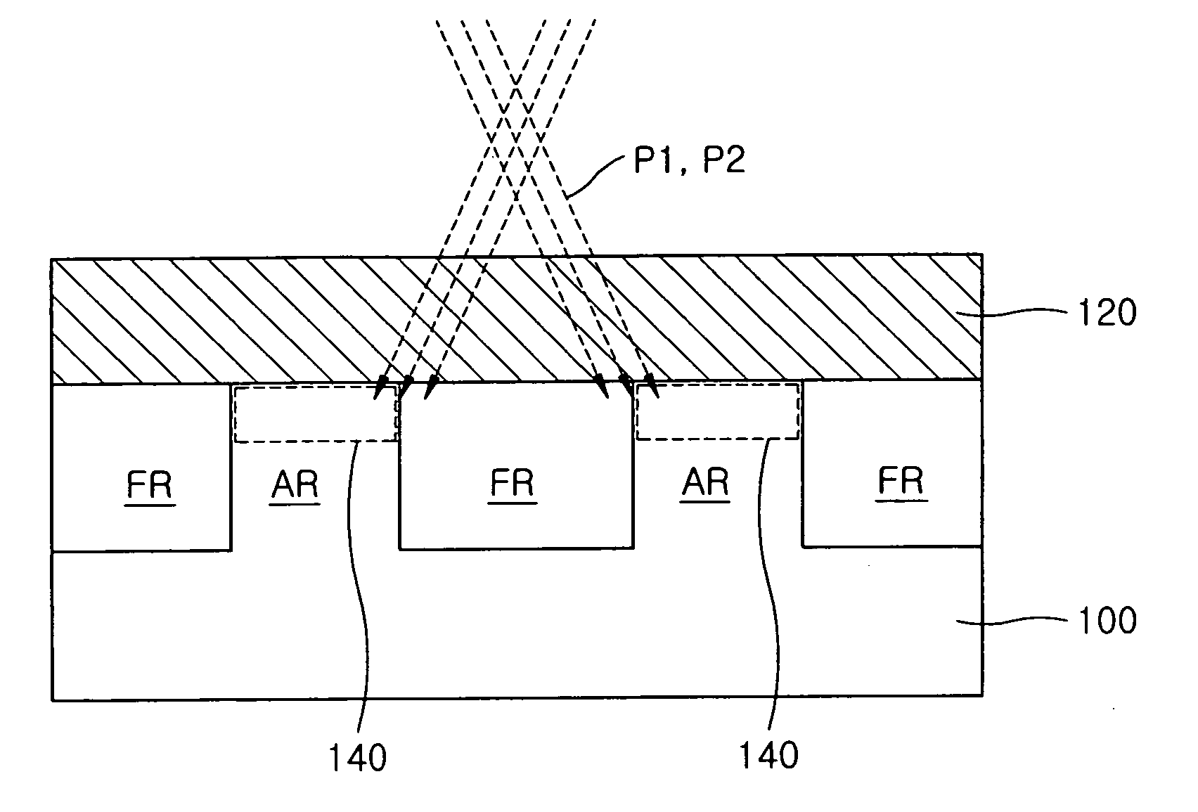
A method of forming an SRAM cell, having two transfer transistors, two driver transistors, and two load devices which are connected with one another in the form of a flip-flop is provided. In particular, after defining an active region and an inactive region on a silicon substrate, a gate electrode conductive pattern of the transistors is formed on the silicon substrate having the active region and the inactive region formed therein along a channel width direction (X-axis direction). Then, after forming a pocket ion implantation region under the conductive pattern, by performing a photolithography process on the conductive pattern along a channel length direction (Y-axis direction), the gate electrodes of the transistors are formed. Even though the gate electrodes are misaligned, impurities for pocket ion implantation are not injected into the gate extension along the channel width direction.

Description

BACKGROUND OF THE INVENTION [0001] This application claims the priority of Korean Patent Application No. 10-2004-0085799, filed on Oct. 26, 2004, in the Korean Intellectual Property Office, the disclosure of which is incorporated herein in its entirety by reference. [0002] 1. Field of the Invention [0003] The present invention relates to a method of forming a memory cell of a semiconductor device, and more particularly, a method of forming an SRAM cell of an SRAM device. [0004] 2. Description of the Related Art [0005] Generally, a static random access memory (SRAM) has the characteristics of high operation speed and low power consumption in comparison with a dynamic random access memory (DRAM), because the SRAM does not need refresh operations. Therefore, the SRAM is widely used for a cache memory of a computer or portable electronic products. The unit cell of the SRAM device is composed of a pair of driver transistors, a pair of transfer transistors, and a pair of load devices. [00...

Claims


Application Information

Patent Timeline
Patent Type & Authority Applications(United States)
IPC IPC(8): H01L21/8238H01L21/425
CPCH01L21/26586H01L27/11H01L27/1104H10B10/00H10B10/12H01L21/265H10B99/00
Inventor JUNG, HYUCK-CHAIYANG, HYEONG-MO
Owner SAMSUNG ELECTRONICS CO LTD
Learn More