Threshold voltage mismatch compensation sense-amplifiers for static random access memories with multiple differential inputs

a random access memory and threshold voltage mismatch technology, applied in the field of sense amplifiers, can solve the problems of different discharging speeds at opt and opc, threshold voltage mismatch between sensing transistors mnb, and low-voltage operation

Inactive Publication Date: 2016-07-14
SACHDEV MANOJ
View PDF1 Cites 9 Cited by
  • Summary
  • Abstract
  • Description
  • Claims
  • Application Information

AI Technical Summary

Benefits of technology

[0014]This invention relates to sense amplifiers for semiconductor memories. The disclosed embodiments in the inventio

Problems solved by technology

This imbalance causes different discharging speeds at OPT and OPC from the precharged voltage.
At this time, the differential voltage at bitlines connected to OPC and OPT creates an imbalance between overdrive voltage (VGS−VT) of latching transistors that leads to regenerative feedback and signal amplification.
One of the problems with the sense amplifier illustrated in FIG. 3 is the threshold voltage mismatch between

Method used


Image

  • Threshold voltage mismatch compensation sense-amplifiers for static random access memories with multiple differential inputs
  • Threshold voltage mismatch compensation sense-amplifiers for static random access memories with multiple differential inputs
  • Threshold voltage mismatch compensation sense-amplifiers for static random access memories with multiple differential inputs

Examples


Embodiment Construction

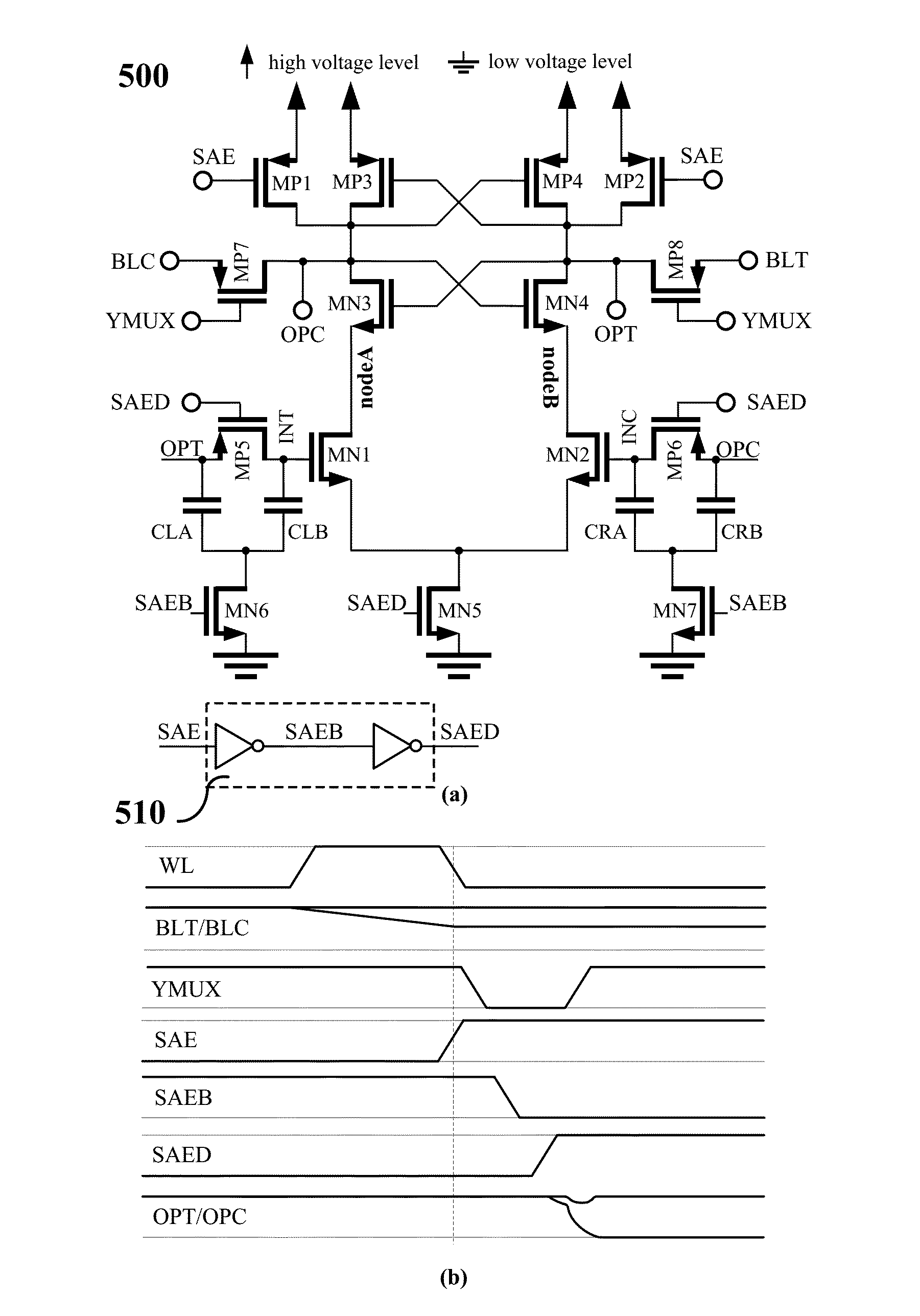
[0030]For convenience, like structures in drawings will be referenced by like numerals in the description. In the present embodiment, the preferred high voltage level or logic 1 is VDD and the preferred low voltage level or logic 0 is ground.

[0031]FIG. 5 shows an embodiment in accordance with the invention. The schematic in FIG. 5(a) has MN3, MN4, MP3, and MP4 as latching transistors formulating the latch with OPT and OPC as input-output nodes of the latch. Two PMOS transistors, MP1 and MP2, selectively couple nodes OPC and OPT to VDD when the sense enable signal (SAE) is low. Transistors MN3 and MN4 are the main sensing transistors of the latch because when the sensing operation starts transistors MP3 and MP4 are off and play a minor role in the operation. Gates of transistors MN1, and MN2 are also selectively coupled to nodes OPT and OPC respectively. These two transistors form a half latch and deemed as auxiliary sensing transistors. A two transistor, MP5 and MN6, and two capacit...


PUM


Abstract

Sense amplifier configurations for memories are described. In these configurations, the differential inputs are boosted proportional to the respective bitline voltage enabling a low-voltage, reliable, faster sense amplifier operation. Disclosed sense amplifiers are also capable of compensating the threshold mismatch between the sensing transistors.

Description

[0001]This application claims the benefit of priority of U.S. Provisional Patent Application No. 61 / 959,701 filed Aug. 30, 2013 which is incorporated herein by reference in its entirety.TECHNICAL FIELD OF INVENTION[0002]This invention relates to the circuit technology associated with sense amplifiers in semiconductor memories. The proposed sense amplifier topology offers reliable, faster sensing capabilities. Some of the embodiments also have desired low-voltage operation.BACKGROUND OF THE INVENTION[0003]On chip Static Random Access Memories (SRAMs) are critical component of the modern system-on-a-chip (SOC) solutions. As CMOS technology has scaled into deep nanometric regime, the density of static random access memory (SRAM) has increased manifolds. As a consequence, for the same die area, density of SRAM bit-cells has increased and there is a great motivation to improve reliability, yield and performance of dense SRAM arrays.[0004]A typical SRAM array is organized in multiple rows...

Claims


Application Information

Patent Timeline
IPC IPC(8): G11C11/419
CPCG11C11/419
Inventor SACHDEV, MANOJSHAH, JASPAL SINGH
Owner SACHDEV MANOJ
Why Eureka
Try Eureka