

Display device and method for manufacturing the same
a technology of display device and manufacturing method, which is applied in the field of display device, can solve the problems of heat resistance of pure aluminum, and achieve the effects of high image quality, high definition and high reliability of display devi
- Summary
- Abstract
- Description
- Claims
- Application Information
AI Technical Summary
Benefits of technology
Problems solved by technology
Method used
Image

Examples
embodiment mode 1
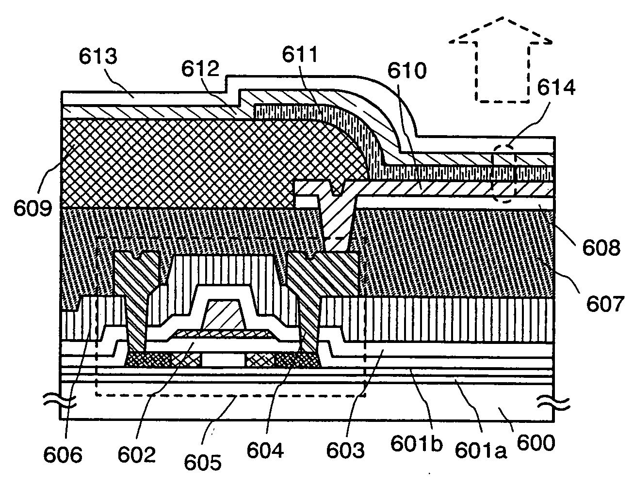
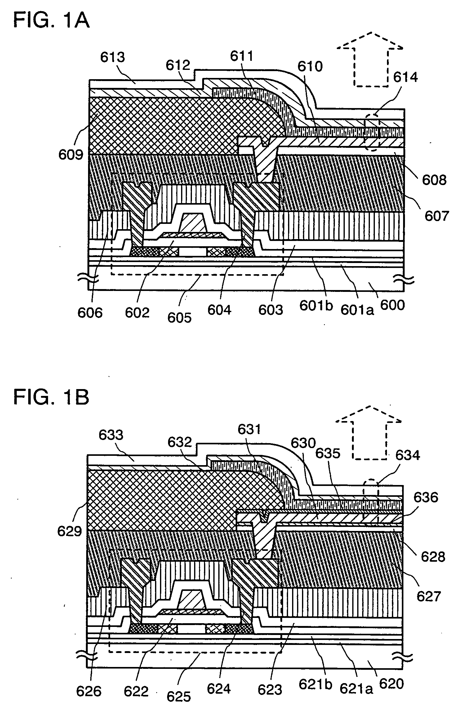
[0047] Display devices of the present embodiment mode will be described with reference to FIGS. 1A and 1B.
[0048] As shown in FIGS. 1A and 1B, a display device according to the present embodiment mode is a top-emission display device in which light is extracted through a sealing substrate. The display devices shown in FIGS. 1A and 1B are examples having light emitting elements of different structures.
[0049] The display device of FIG. 1A includes, over a substrate 600, a base film 601a, a base film 601b, a thin film transistor 605, a gate insulating layer 602, an insulating layer 603, an insulating layer 606, an insulating layer 607, an interlayer film 608, an insulating layer 609 serving as a bank, a first electrode layer 610, an electroluminescent layer 611, a second electrode layer 612, and a protective film 613. The thin film transistor 605 includes a semiconductor layer having an impurity region which serves as a source region and a drain region, a gate insulating layer 602, a ...
embodiment mode 2
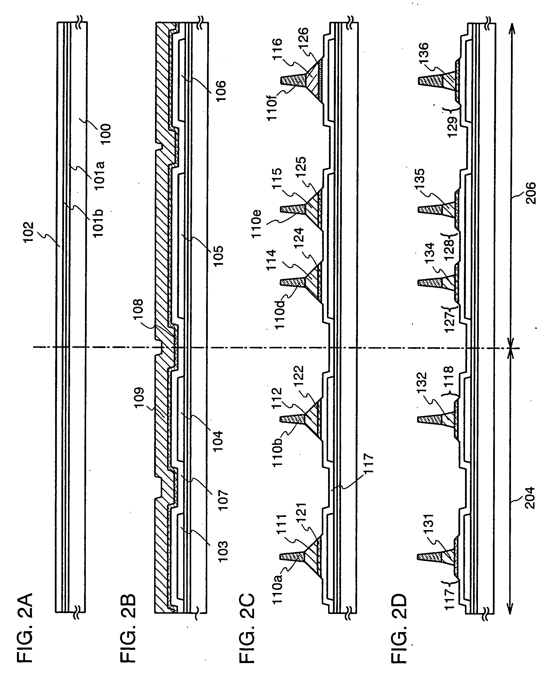
[0093] A manufacturing method of a display device according to this embodiment mode will be described in details with reference to FIGS. 2A to 7B, 16A to 16C, and 17A and 17B.
[0094]FIG. 16A is a top view showing a structure of a display panel according to the invention, including a pixel portion 2701 in which a pixel 2702 is arranged in matrix, a scan line side input terminal 2703, a signal line side input terminal 2704 which are formed over a substrate 2700 having an insulating surface. The number of pixels may be set according to various standards, for example, 1024×768×3 (RGB) in the case of XGA, 1600×1200×3 (RGB) in the case of UXGA, and 1920×1080×3 (RGB) in the case of the use for a full spec high vision display.
[0095] The pixel 2702 is arranged in matrix with a scan line extending from the scan line side input terminal 2703 and a signal line extending from the signal line side input terminal 2704 crossing. Each pixel 2702 is provided with a switching element and a pixel elec...
embodiment mode 3
[0191] Embodiment Mode according to the present invention is described with reference to FIGS. 8A to 10. This embodiment mode will describe an example in which a second interlayer insulating film is not formed in the display device manufactured in Embodiment Mode 1. Therefore, the description of the same portions and the portions having the same function is omitted.
[0192] As shown in Embodiment Mode 1, p-channel thin film transistors 173 to 176 and an insulating film 168 are formed over a substrate 100. A source or drain electrode layer to be connected to a source or drain region of a semiconductor layer is formed in each thin film transistor. A first electrode layer 395 is formed to be in contact with a source or drain electrode layer 172b in the p-channel thin film transistor 176 provided in a pixel portion 206 (FIG. 8A).
[0193] The first electrode layer 395 serves as a pixel electrode, and may be formed from the same material in the same process as the first electrode layer 395 ...
PUM
 Abstract
Description
Claims
Application Information