Self-aligned gated p-i-n diode for ultra-fast switching

US20060091490A1Inactive Publication Date: 2006-05-04TAIWAN SEMICON MFG CO LTD

Image

  • Self-aligned gated p-i-n diode for ultra-fast switching
  • Self-aligned gated p-i-n diode for ultra-fast switching
  • Self-aligned gated p-i-n diode for ultra-fast switching

Examples


Embodiment Construction

[0024] The making and using of the presently preferred embodiments are discussed in detail below. It should be appreciated, however, that the present invention provides many applicable inventive concepts that can be embodied in a wide variety of specific contexts. The specific embodiments discussed are merely illustrative of specific ways to make and use the invention, and do not limit the scope of the invention.

[0025] A manufacturing process of a preferred embodiment of the present invention is discussed. Variations of the preferred embodiments are presented. Like reference numbers are used to designate like elements throughout the various views and illustrative embodiments of the present invention. Each figure number may be followed by a letter A, B or C showing variations of the same process step.

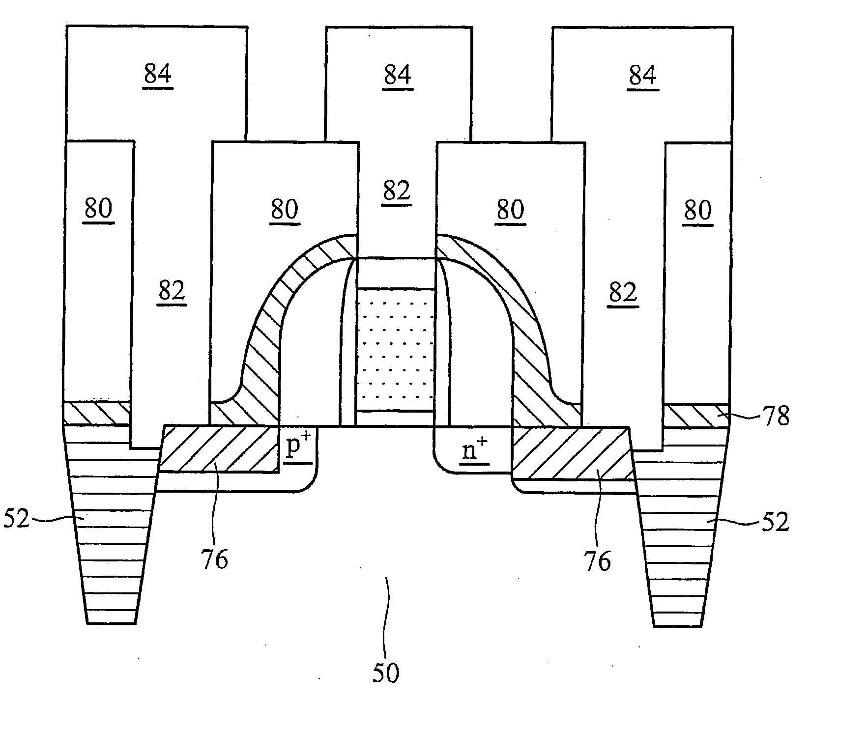
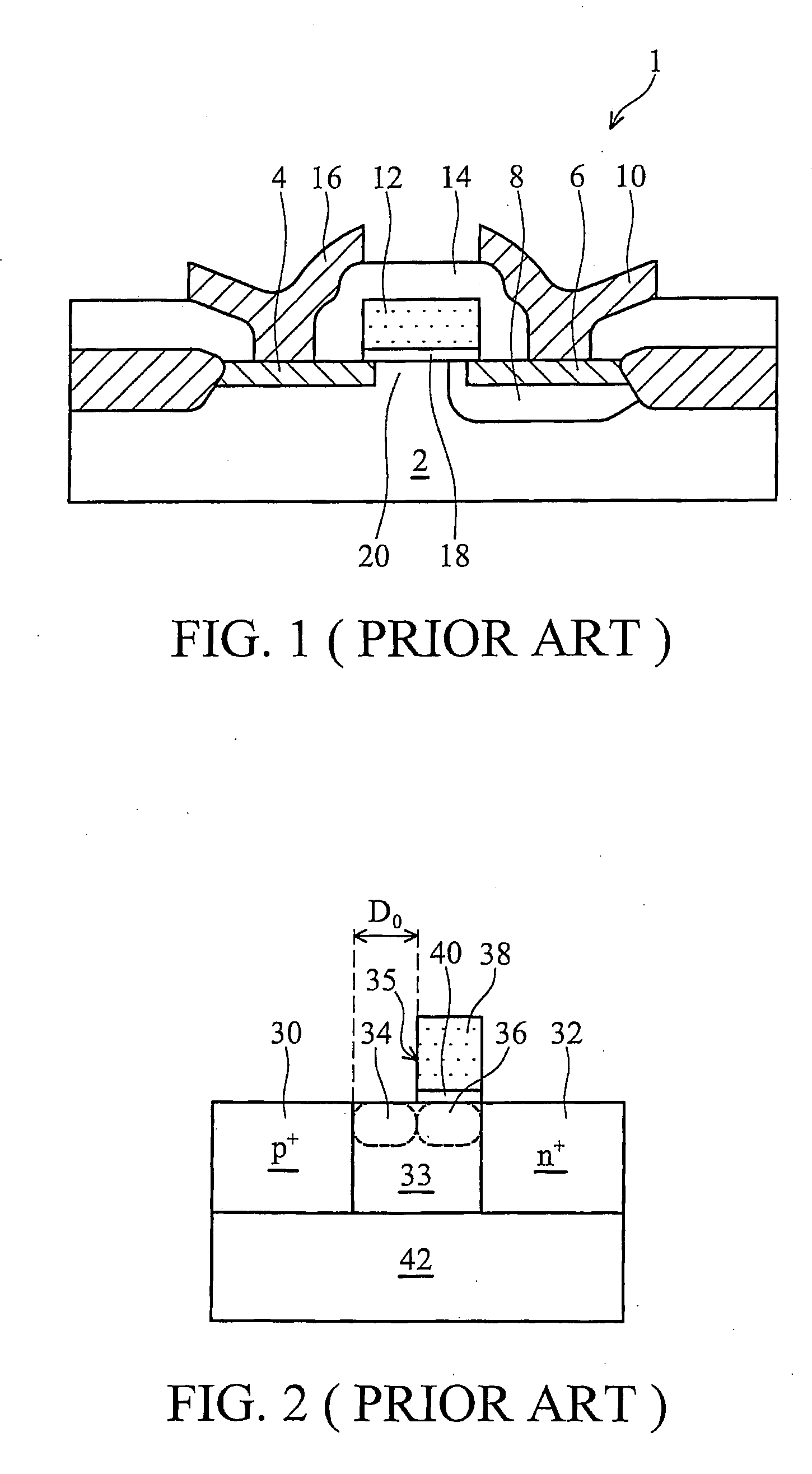
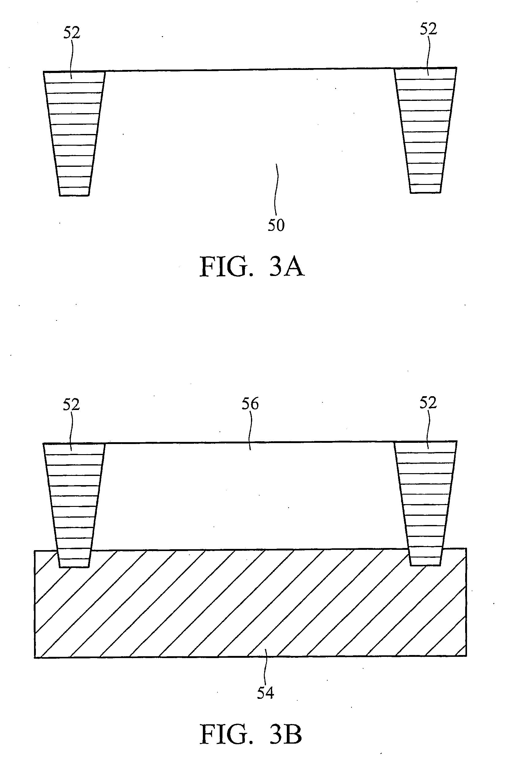
[0026]FIGS. 3 through 10 illustrate a preferred embodiment of a gated p-i-n diode of the present invention. FIG. 3A illustrates shallow trench isolations (STI) 52 formed in a substrate...


PUM


Abstract

A gated p-i-n diode and a method for forming the same. The gated p-i-n diode comprises: a semiconductor substrate; a gate dielectric over the semiconductor substrate; a gate electrode on the gate dielectric; a source gate spacer and a drain gate spacer along respective edges of the gate dielectric and the gate electrode; a source doped with a first type of dopant substantially under the source gate spacer wherein the source has a horizontal distance from a first edge of the gate electrode; a drain doped with the opposite type of the source substantially under the drain spacer and substantially aligned horizontally with a second edge of the gate electrode; a source silicide adjacent the source; and a drain silicide adjacent the drain.

Description

[0001] This application claims the benefit of U.S. Provisional Application No. 60 / 624,631, filed on Nov. 3, 2004, entitled “Self-Aligned Gated p-i-n Diode,” which application is hereby incorporated herein by reference. CROSS-REFERENCE TO RELATED APPLICATIONS [0002] This application relates to co-pending and commonly assigned patent application Ser. No. ______ (TSM04-0925), filed concurrently herewith, entitled “Multi-Level Flash Memory Cell Capable Of Fast Programming.”TECHNICAL FIELD [0003] This invention relates generally to semiconductor devices, and more specifically to gated p-i-n diodes. BACKGROUND [0004] Metal-oxide-semiconductor (MOS) is a dominating technology for integrated circuits at 90 nm technology and beyond. An MOS device can work in three regions depending on gate voltage Vg and source-drain voltage Vds, linear, saturation and sub-threshold. Sub-threshold is a region where Vg is smaller than the threshold voltage Vt. The sub-threshold slope represents the easiness o...

Claims


Application Information

Patent Timeline
04 May 2006
Publication
US20060091490A1
IPC
H01L31/105
CPC
H01L29/7391; H01L29/868
Inventors
CHEN, HUNG-WEI; LEE, WEN-CHIN