Differentially metal doped copper damascenes

a metal doped, damascene technology, applied in the direction of semiconductor devices, semiconductor/solid-state device details, electrical apparatus, etc., can solve the problems of increasing the size of existing voids, degrading (increasing) the electrical resistivity of copper, and exhibiting certain processing problems

Inactive Publication Date: 2006-05-04
TAIWAN SEMICON MFG CO LTD
View PDF2 Cites 36 Cited by
  • Summary
  • Abstract
  • Description
  • Claims
  • Application Information

AI Technical Summary

Problems solved by technology

Copper, however, has exhibited certain processing problems that must be overcome to achieve a mature copper metal interconnect semiconductor processing technology.
Frequently, such subsequent thermal processes may induce copper diffusion including the formation of hillocks or protrusions on the copper surface portion, as well as forming voids or increasing the size of existing voids within the deposited copper interconnect.
Other problems associated with copper filled semiconductor features include the undesired growth of copper grain size in s

Method used


Image

  • Differentially metal doped copper damascenes
  • Differentially metal doped copper damascenes
  • Differentially metal doped copper damascenes

Examples


Embodiment Construction

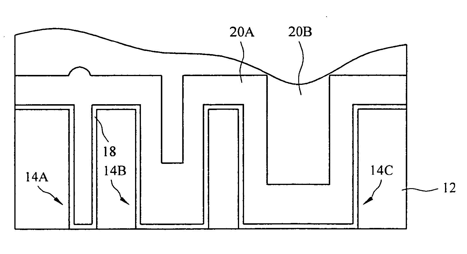
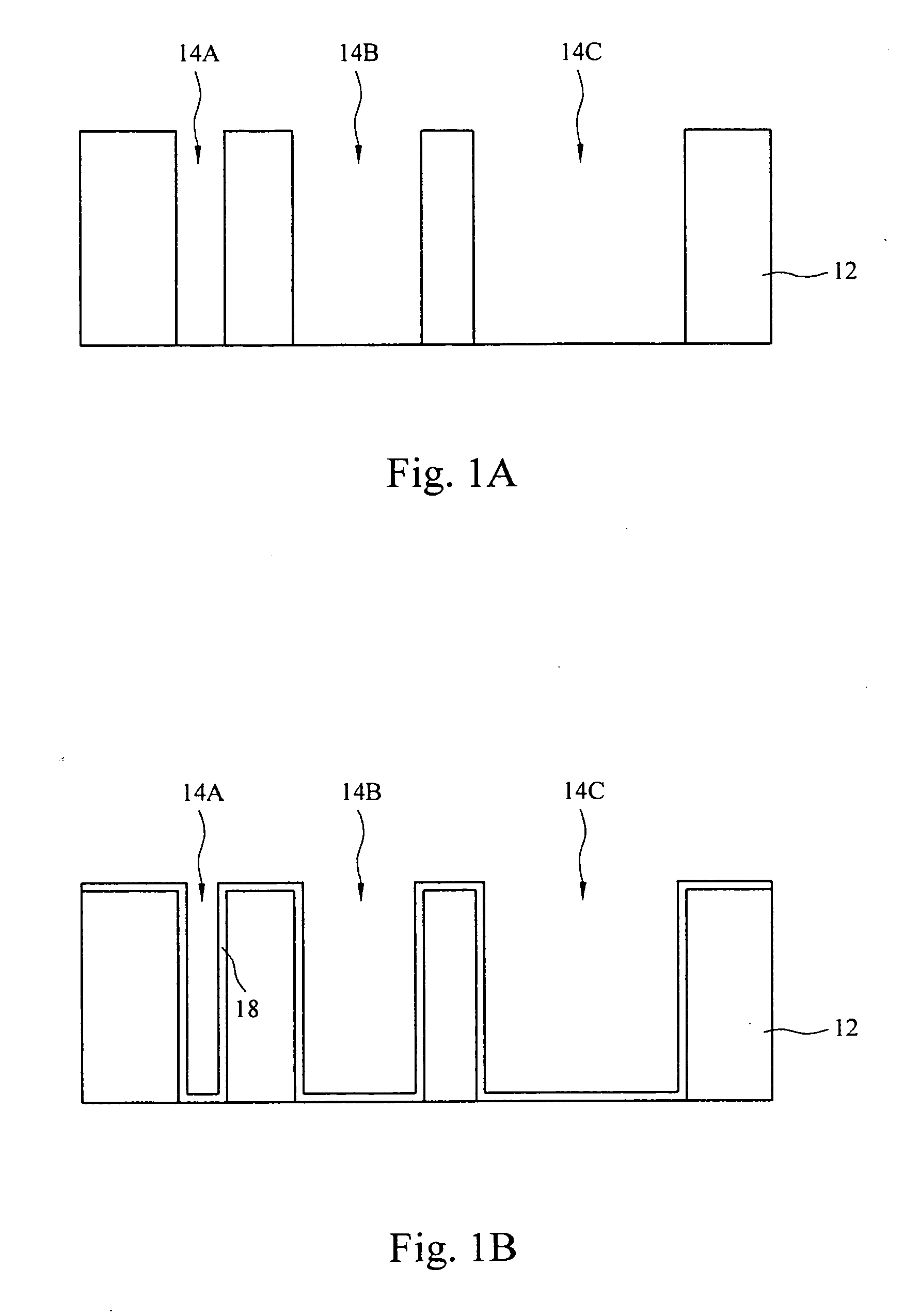
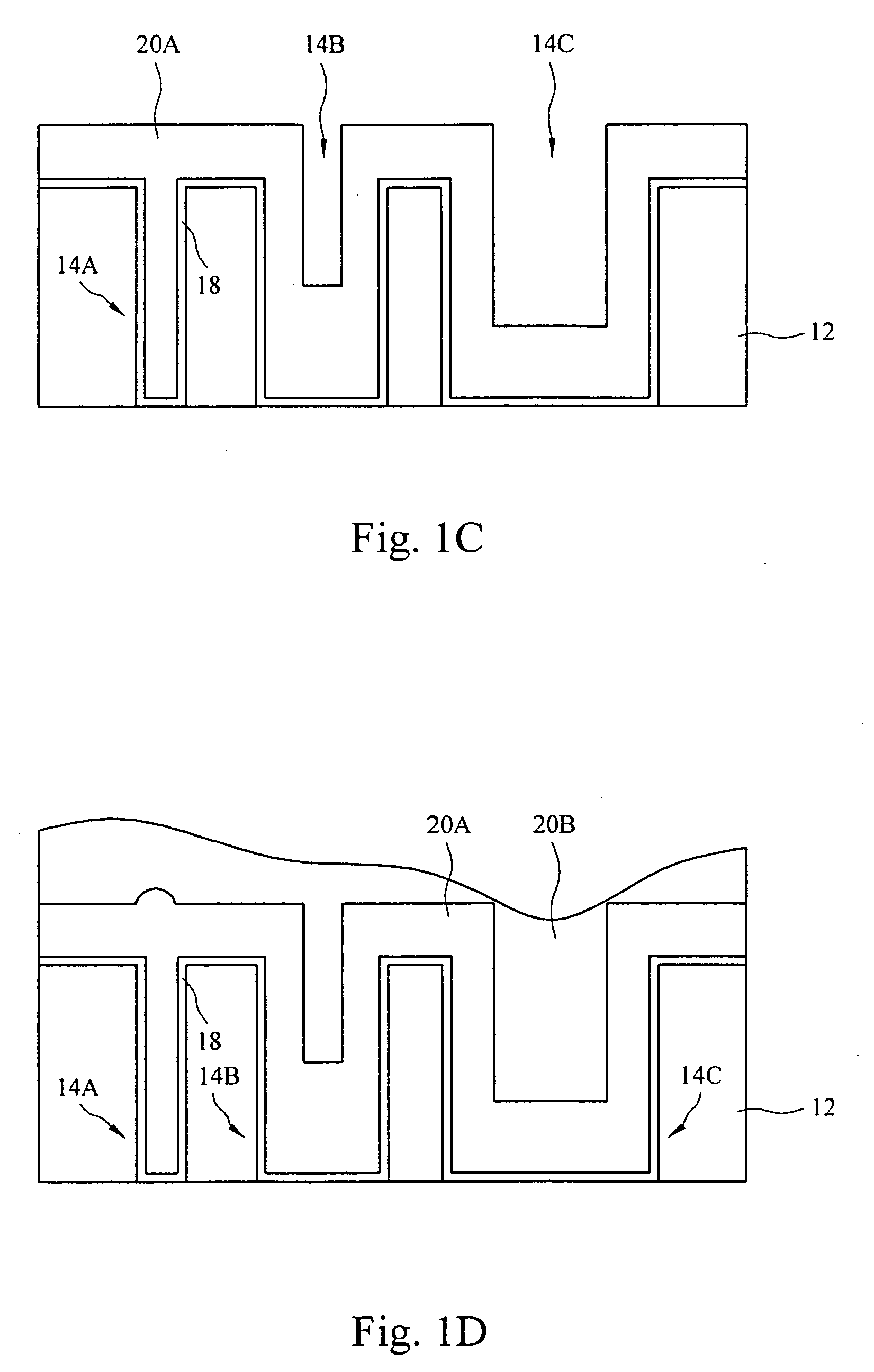
[0015] Although the method of the present invention is explained with reference to copper interconnect (trench) lines having respectively different widths in a single metallization layer, it will be appreciated that the method may be applied to any copper filled feature including single damascene features such as bonding pads, interconnect lines, and vias as well as dual damascene features, for example an interconnect lines having a via portion underlying the interconnect line portion. For example, the method of the present invention advantageously suppresses copper diffusion in larger width damascenes wile maintaining a desired resistivity in narrower width damascenes by advantageously forming copper portions having different metal doping concentrations in different damascene width sizes in a single metallization layer in a multi-step electro-chemical deposition (ECD) process. According to an aspect of the invention, copper damascene structures having different widths in a metalliz...


PUM

PropertyMeasurementUnit
Widthaaaaaaaaaa
Widthaaaaaaaaaa
Widthaaaaaaaaaa

Abstract

A method of forming a copper filled semiconductor feature having improved bulk properties including providing a semiconductor process wafer having a process surface including an opening for forming a semiconductor feature; depositing at least one metal dopant containing layer over the opening to form a thermally diffusive relationship to a subsequently deposited copper layer; depositing said copper layer to substantially fill the opening; and, thermally treating the semiconductor process wafer for a time period sufficient to distribute at least a portion of the metal dopants to collect along at least a portion of the periphery of said copper layer including a portion of said copper layer grain boundaries.

Description

FIELD OF THE INVENTION [0001] This invention generally relates to methods for forming copper filled semiconductor features and more particularly to a method for producing copper filled semiconductor feature in a metallization layer to produce differentially metal (impurity) doped copper damascenes, depending on the width of the copper damascene, to improve a copper electromigration resistance including void formation while maintaining an acceptably low resistivity. BACKGROUND OF THE INVENTION [0002] Sub-micron multi-level metallization is one of the key technologies for ultra large scale integration (ULSI). The multilevel interconnects that lie at the heart of this technology require formation of conductive interconnect features having a variety of widths, including dual damascenes and interconnect lines. Reliable formation of these interconnect features is critical to the functioning and reliability of the semiconductor device formed. [0003] Copper and copper alloys have become the...

Claims


Application Information

Patent Timeline
IPC IPC(8): H01L23/52H01L21/4763
CPCC25D3/58C25D5/022C25D5/10H01L21/2885H01L21/76816H01L21/76877C25D7/123
Inventor LIN, CHUN-CHIEHCHOU, SHIH-WEITSAI, MINGHSING
Owner TAIWAN SEMICON MFG CO LTD
Why Eureka
Try Eureka