Method for manufacturing an electrode plate with improved reliability

Inactive Publication Date: 2006-05-04
IND TECH RES INST
View PDF2 Cites 0 Cited by
  • Summary
  • Abstract
  • Description
  • Claims
  • Application Information

AI Technical Summary

Benefits of technology

[0006] The primary objective of the present invention is to provide a method of manufacturing an electrode plate with improved reliability. The method can improve reliability of an electrode plate such that the conductive part of the electrode plate will not break down and surroundings of the luminescence material of the electrode plate will not occur damages or broken lines when high current density is led into the electrode plate.
[0007] To achieve the foregoing objective, the method of manufacturing an electrode plate with improved reliability comprises the following steps: (a) providing a glass substrate; (b) spreading an Indium Tin Oxide (ITO) layer on a specific area of the glass substrate; (c) exposing and developing the ITO layer; and (d) spreading at least a thick film conductive layer on the ITO layer. In which, the step of spreading a thick film conductive layer is processed by a thick film screen printing process so that the manufactured thickness of the thick film conductive layer can sustain high current density without damages.
[0008] To make the examiner easier to understand the objective, structure, innovative features, and function of the invention, preferred embodiments together with accompanying drawings are illustrated for the detailed description of the invention.

Problems solved by technology

When the display is required to increase the voltage to produce more electrons to hit the phosphor powders and result in brighter luminescence or when the luminescence area of the display increases, the conductive part which collects electrons flow on the electrode plate can not bear and will break down such that the electrons can not flow into the display and the display will be invalidated.
Therefore, the design for an electrode plate regarding whether the display can sustain high electrons flow is an important issue.
However, the prior arts used a thin film process so that the thickness of the metal layer and the ITO layer is insufficient for high electronics flow and causes the display to break down.
However, the material of the frame pattern is not conductive and the frame pattern is manufactured by a thin film process so that the frame pattern has no effect of reducing current density.

Method used


Image

  • Method for manufacturing an electrode plate with improved reliability
  • Method for manufacturing an electrode plate with improved reliability
  • Method for manufacturing an electrode plate with improved reliability

Examples


Embodiment Construction

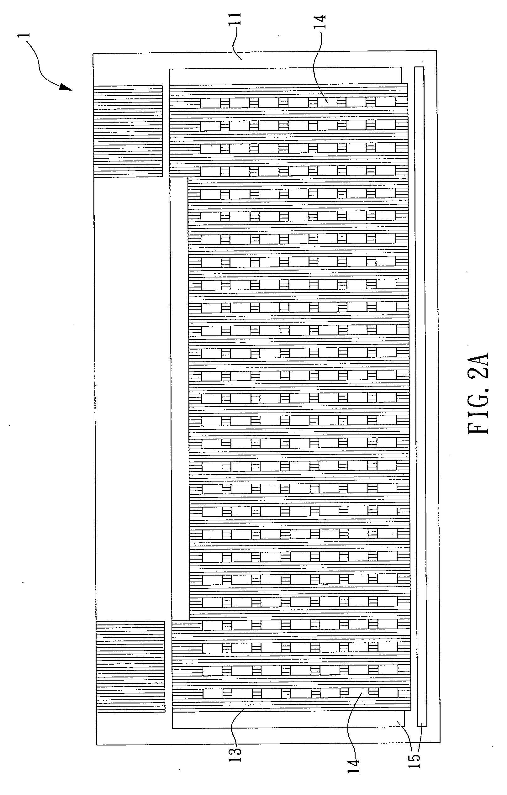
[0013]FIG. 2A and FIG. 2B is a top-view diagram and a cross sectional diagram of an electrode plate with improved reliability of the present invention, respectively, wherein the electrode plate 1 is a non-backlight anode plate which comprising a glass substrate 11, an ITO layer 12, a thick film conductive layer 13, a luminescence material 14 and a metal layer 16. The ITO layer 12 is stacked on an area 111 of the glass substrate 11 and the metal layer 16 is stacked on the ITO layer 12. The thick film conductive layer 13 is spread on the metal layer 16 and the luminescence material 14 is stacked on an area 112 of the glass substrate 11, wherein the area 111 and the area 112 are independent and non-overlapped ones. The ITO layer 12 and the metal layer 16 form the conductive layer 15.

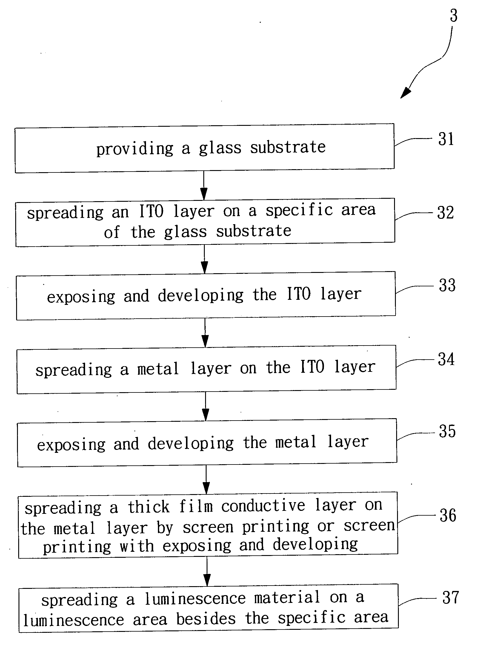
[0014]FIG. 3 is a flowing chart of manufacturing an anode plate according to the present invention. The anode plate manufacturing process 3 comprises steps 31-37, wherein step 31 is a step of providing a g...


PUM


Abstract

A method for manufacturing an electrode plate with improved reliability, comprising: (a) providing a glass substrate; (b) spreading an Indium Tin Oxide (ITO) layer on a specific area of the glass substrate; (c) exposing and developing the ITO layer; and (d) screen printing at least a thick film conductive layer on the ITO layer.

Description

FIELD OF THE INVENTION [0001] The present invention relates to a method of manufacturing an electrode plate, more particularly to a method of manufacturing an electrode plate by using a process of thick film screen printing. BACKGROUND OF THE INVENTION [0002] The luminescence principle of a field emission display is that using an electric field in a vacuum condition to attract out electrons at material tips thus the field emission electrons leaving the cathode plate, being accelerated by a positive voltage on the anode plate and hitting the phosphor powders on the anode plate to emit light, and the electrons received on the electrode plate returning to the circuit via the conductive part of the electrode plate. When the display is required to increase the voltage to produce more electrons to hit the phosphor powders and result in brighter luminescence or when the luminescence area of the display increases, the conductive part which collects electrons flow on the electrode plate can ...

Claims


Application Information

Patent Timeline
IPC IPC(8): B05D5/06B05D5/12
CPCH01J9/14H01J9/20H01J31/127H01J63/02H01M4/0402H01M4/0419Y02E60/10
Inventor LIN, BIING-NANHSIAO, MING-CHUNLEE, CHUN-TAOLIN, WEI-YI
Owner IND TECH RES INST
Why Eureka
Try Eureka