

Pulse generation circuit
a generation circuit and pulse technology, applied in the direction of pulse technique, generating/distributing signals, instruments, etc., can solve the problems of inconstant output, affecting the speed of the pulse, and increasing the size of the timing control unit, so as to achieve high (hi) voltage levels
- Summary
- Abstract
- Description
- Claims
- Application Information
AI Technical Summary
Benefits of technology
Problems solved by technology
Method used
Image

Examples
first embodiment
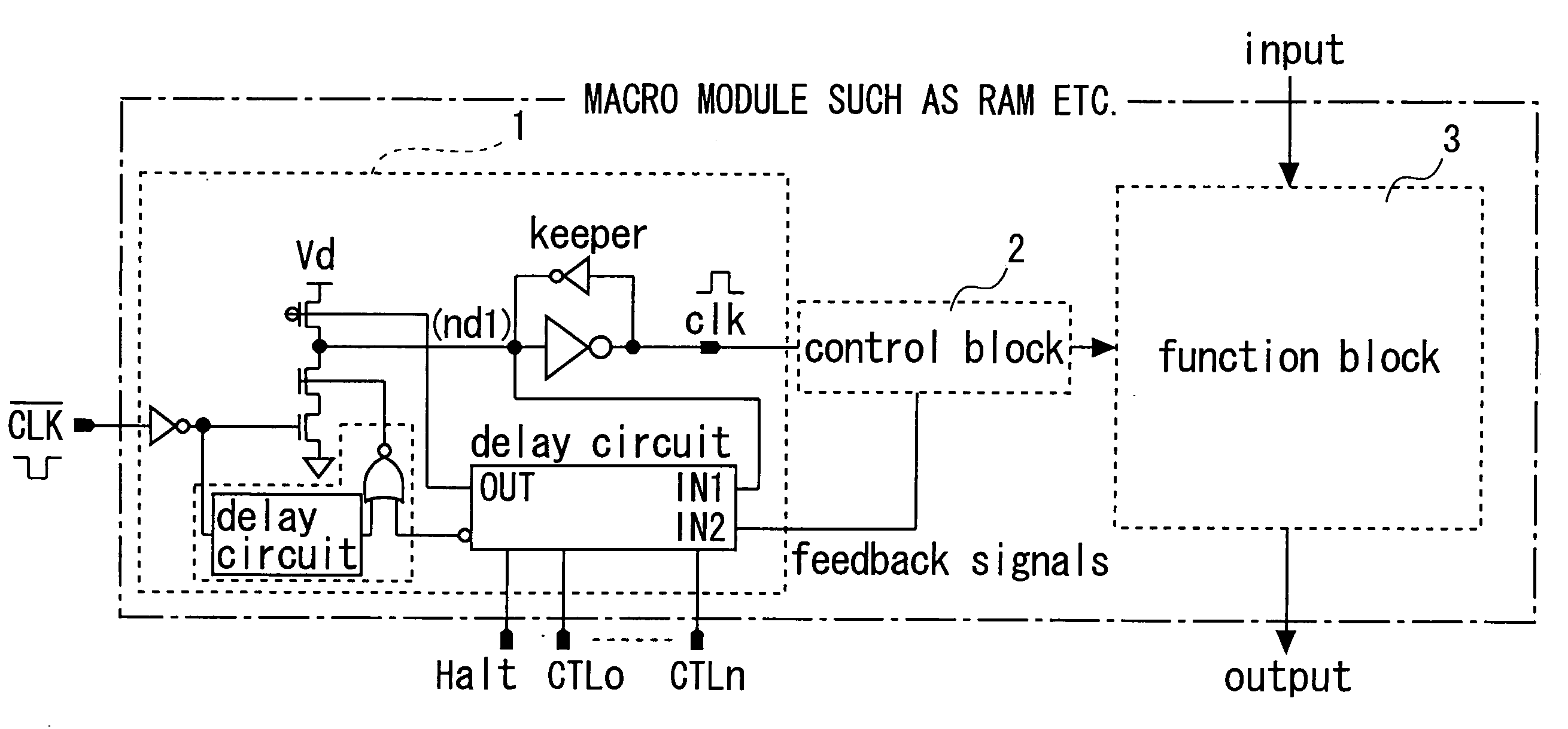
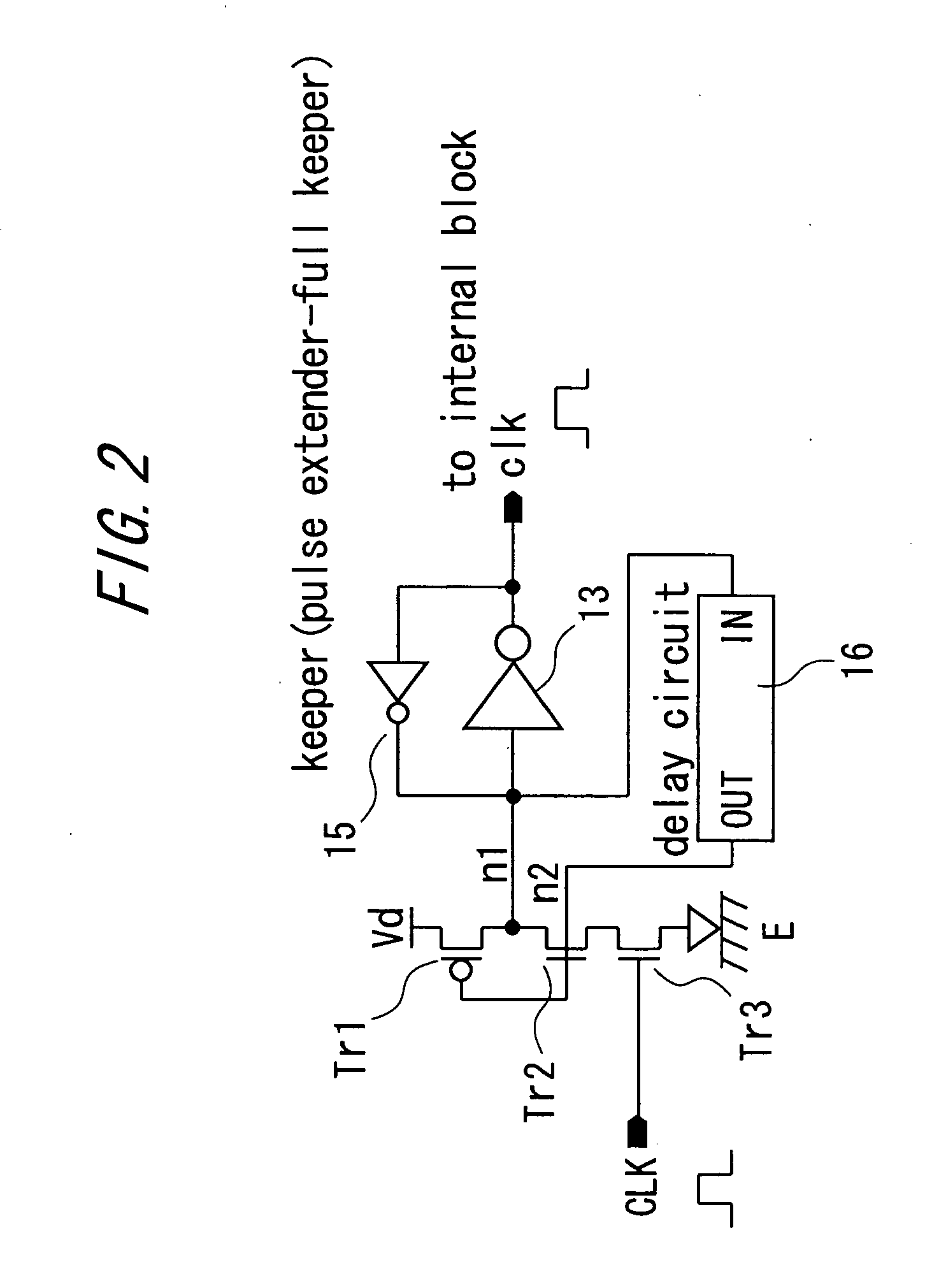
[0048]FIG. 2 shows the pulse generation circuit as a first embodiment of the present invention.
[0049] The pulse generation circuit 1 in the first embodiment is constructed of a P-type MOS (Metal Oxide Semiconductor) transistor Tr1, first and second N-type MOS transistors Tr2, Tr3, a delay circuit 16, an inverter 13 and a keeper 15.
[0050] A drain electrode of the P-type MOS transistor Tr1 is connected to a first power source line. A drain electrode of the first N-type MOS transistor Tr2 is connected to a source electrode of the P-type MOS transistor Tr1.
[0051] A drain electrode of the second N-type MOS transistor Tr3 is connected to a source electrode of the first N-type MOS transistor Tr2, a gate electrode of the second N-type MOS transistor Tr3 is connected to an input line CLK to which the input pulse signal is inputted, and a source electrode thereof is connected to a second power source line. In this first embodiment, the first power source line is a power source line supplie...
second embodiment
[0067] The first embodiment takes the configuration that the input pulse signal is inputted to the second N-type MOS transistor Tr3, and the output of the delay circuit 16 is inputted to the P-type MOS transistor Tr1 and to the first N-type MOS transistor Tr2 (corresponding to claim 1), however, another configuration shown in FIG. 6 is also available, wherein the layout of the N-type MOS transistors is exchanged (corresponding to claim 2).
[0068] Specifically, in the pulse generation circuit 1 in the second embodiment, the drain electrode of the P-type MOS transistor Tr1 is connected to the first power source line, a drain electrode of a first N-type MOS transistor Tr4 is connected to the source electrode of the P-type MOS transistor Tr1, and a gate electrode of the first N-type MOS transistor Tr4 is connected to the input line to which the input pulse signal is inputted. Further, a drain electrode of a second N-type MOS transistor Tr5 is connected to the source electrode of the fir...
third embodiment
[0073] In the first embodiment discussed above, the input terminal of the delay circuit is connected to the source electrode of the P-type MOS transistor Tr1 and to the drain electrode of the first N-type MOS transistor Tr2, i.e., to the node n1, however, the present invention is not limited to this connection. For example, in a third embodiment, as shown in FIG. 7, an input terminal of a delay circuit 12 is connected to the output line clk. This delay circuit 12 takes a configuration that an odd number of inverters are connected in series. Other configurations are the same as those in the first embodiment discussed above, and hence the repetitive explanations are omitted in a way that marks the same components with the same numerals and symbols.
[0074] Namely, in the pulse generation circuit 1 in the third embodiment, the voltage level of the node n1 is inverted by the inverter 13 and is thus inputted to the delay circuit 12, and consequently this voltage level is, after being inve...
PUM
 Abstract
Description
Claims
Application Information