Plasma processing apparatus

a processing apparatus and plasma technology, applied in the direction of coatings, chemical vapor deposition coatings, electric discharge tubes, etc., can solve the problems of power level, reliability degradation of semiconductor devices, and difficulty in diversely matching elements, so as to improve plasma damage

Inactive Publication Date: 2006-05-18
SAMSUNG ELECTRONICS CO LTD
View PDF4 Cites 99 Cited by
  • Summary
  • Abstract
  • Description
  • Claims
  • Application Information

AI Technical Summary

Benefits of technology

[0016] In order to solve the aforementioned problems, the present invention provides a plasma processing

Problems solved by technology

However, the increase in the power level and the maximization of the plasma density cause a problem.
Accordingly, the degradation of a gate oxide film is caused and thus the reliability of the semiconductor device deteriorates (hereinafter referred to as “plasma damage”).
However, it is difficult to diversely correspond to an element which is not previ

Method used


Image

  • Plasma processing apparatus
  • Plasma processing apparatus
  • Plasma processing apparatus

Examples


Embodiment Construction

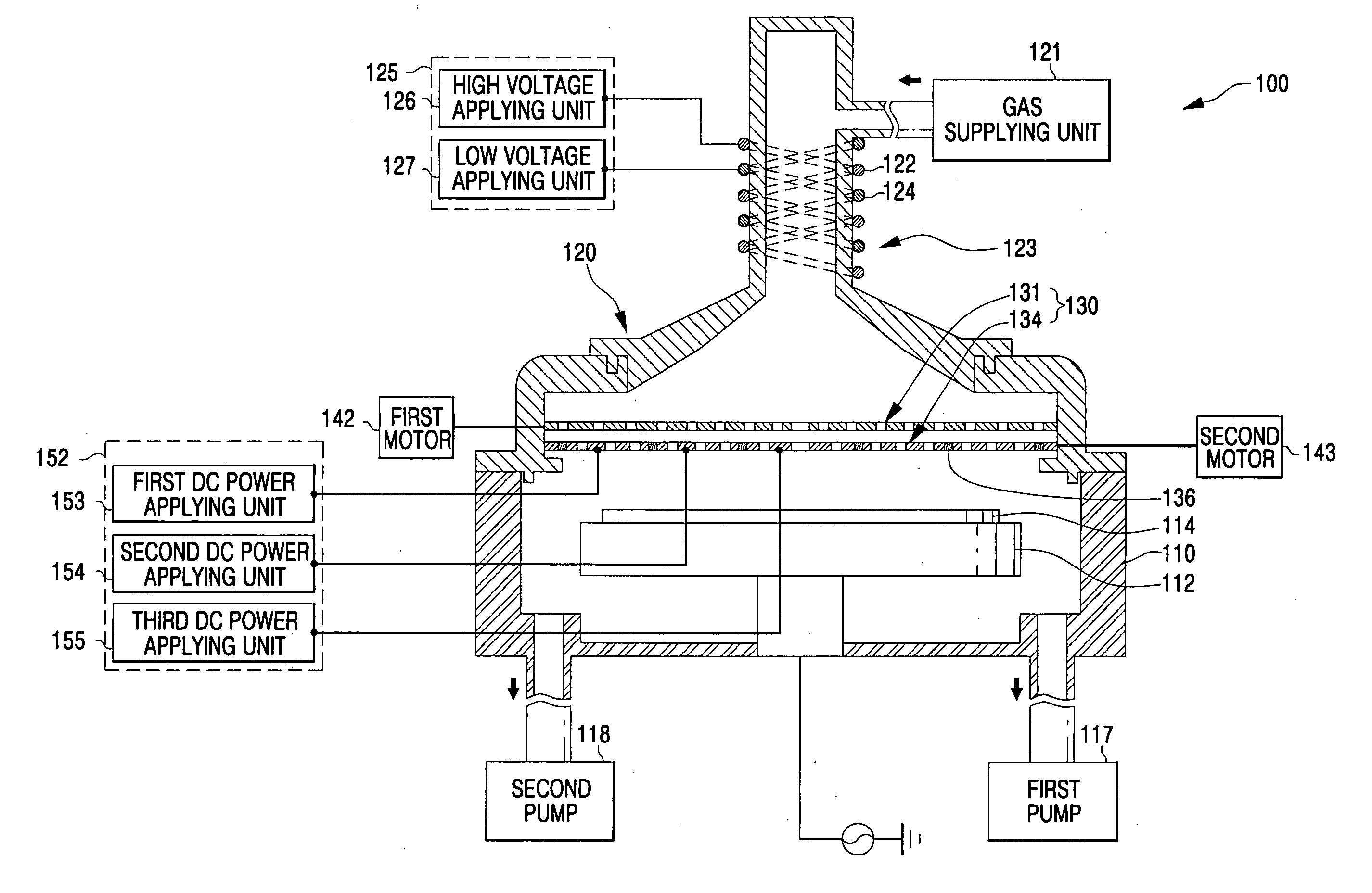
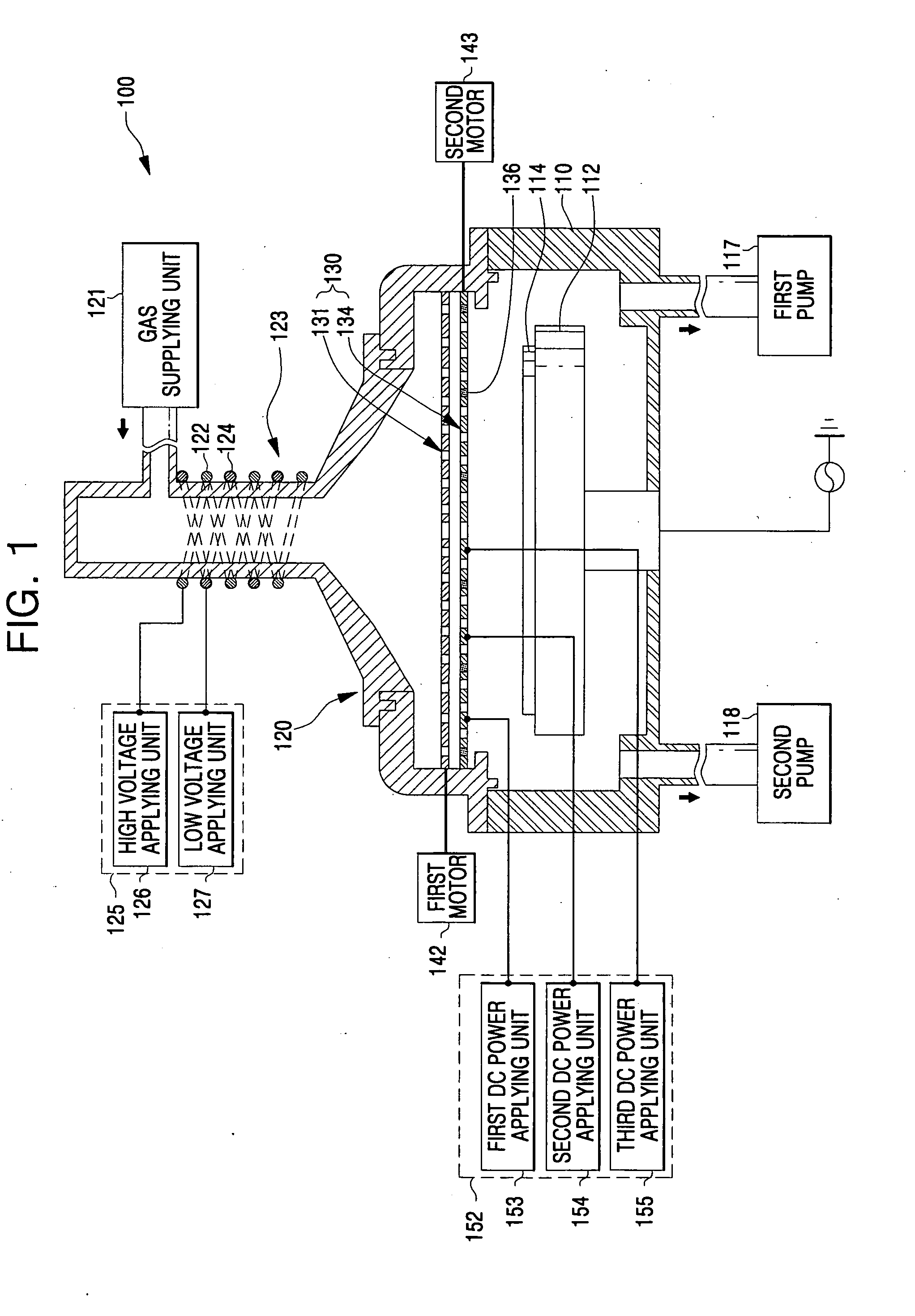
[0028] Now, exemplary embodiments of a plasma processing apparatus of the present invention will be described in detail with reference to FIGS. 1 through 4.

[0029] First, referring to FIG. 1, the plasma processing apparatus 100 according an embodiment of to the present invention includes a process chamber 110 for forming a plasma processing space, a plasma chamber 120 connected to the upper portion of the process chamber 110, and generates and injects plasma into the plasma processing space such that a substrate 114, such as a wafer, is processed. A screen is interposed between the process chamber 110 and the plasma chamber 120 and blocks plasma ions injected from the plasma chamber 120. An ion trap prevents the surface of the substrate 114 from being damaged by the plasma ions into the process chamber 110. A controller (not shown) controls the entire plasma processing apparatus.

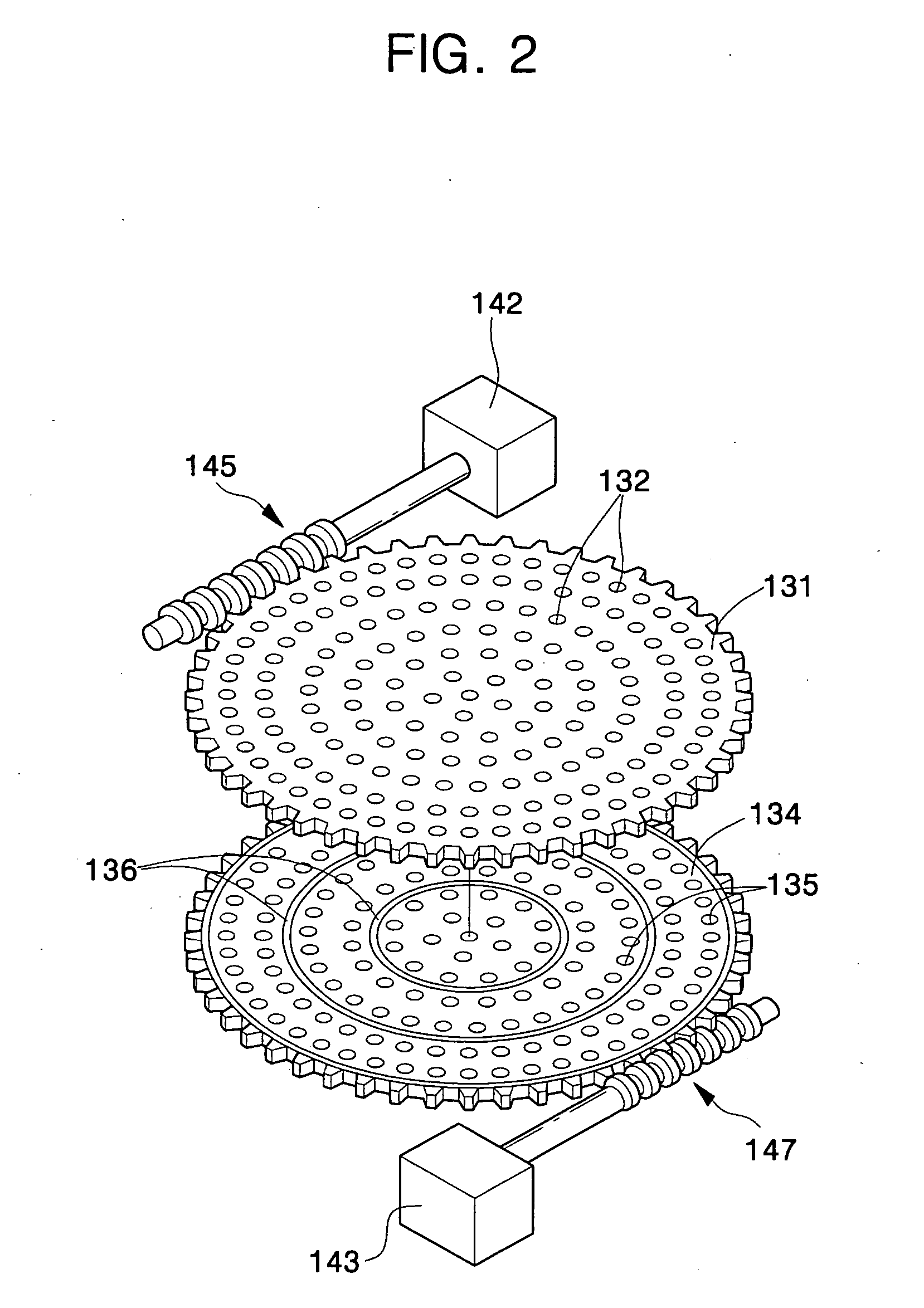
[0030] A substrate holder 112 is installed within the process chamber 110 such that the substrate 114 wh...


PUM

PropertyMeasurementUnit
Poweraaaaaaaaaa
Sizeaaaaaaaaaa

Abstract

A plasma processing apparatus comprising: a process chamber for defining a plasma processing space in which a substrate holder for mounting a substrate thereon is installed; a plasma chamber in communication with an upper portion of the process chamber to generate and inject plasma into the plasma processing space such that the substrate is processed; a screen interposed between the process chamber and the plasma chamber to block plasma ions from being injected from the plasma chamber; and an ion trap for protecting the surface of the substrate from damage due to the injected plasma ion.

Description

[0001] This application claims the priority of Korean Patent Application No. 2004-92685, filed on Nov. 12, 2004, in the Korean Intellectual Property Office, the disclosure of which is incorporated herein in its entirety by reference. BACKGROUND OF THE INVENTION [0002] 1. Field of the Invention [0003] The present invention relates to a plasma processing apparatus and more particularly to an inductively coupled plasma (ICP) processing apparatus. [0004] 2. Description of the Related Art [0005] Recently, a low pressure and low temperature plasma technology has been widely used in the manufacture of semiconductor devices and flat display panels. The Plasma technology is used to etch or deposit certain materials on the surfaces of wafers for semiconductor devices or liquid crystal display (LCD) panels. Particularly, in an etching or thin film deposition process for manufacturing highly integrated semiconductor devices, the usage of plasma equipment has increased. [0006] The most important...

Claims


Application Information

Patent Timeline
IPC IPC(8): C23F1/00C23C16/00
CPCC23C16/452C23C16/507H01J37/32357H01J37/32495H01J37/32623H01L21/02
Inventor KIM, DO-HYEONG
Owner SAMSUNG ELECTRONICS CO LTD
Why Eureka
Try Eureka