Member for semiconductor device

a technology for semiconductor devices and members, applied in semiconductor devices, semiconductor/solid-state device details, electrical devices, etc., can solve the problems of insufficient bonding strength between the naturally oxidized film and the resin, the alloy or composite itself constituting the member cannot have corrosion resistance, and the bonding strength cannot be obtained. , to achieve the effect of improving the bonding strength, excellent resin bonding properties, and high resin bonding strength

Inactive Publication Date: 2006-05-18
SUMITOMO ELECTRIC IND LTD
View PDF10 Cites 6 Cited by
  • Summary
  • Abstract
  • Description
  • Claims
  • Application Information

AI Technical Summary

Benefits of technology

[0017] In consideration of the aforementioned conventional problems, an object of the present invention is to provide a member for a semiconductor device made of an alloy or composite of Cu—W, Cu—Mo, Al—SiC, Si—SiC, etc. wherein the member has an excellent resin bonding property capable of improving resin bonding strength at the time the member for a semiconductor device being bonded to another member with resin and maintains a high resin bonding strength even after various reliability tests, such as a thermal cycling test, are performed, and to provide a semiconductor device employing the member.

Problems solved by technology

However, an alloy or composite itself constituting the member does not have corrosion resistance.
The problem with the resin bonding method is that, since Ni or Au conventionally used as the plating layer has an inferior resin bonding property, a required bonding strength cannot be obtained.
However, in Al and Cu, the bonding strength between the naturally oxidized film and the resin is not sufficient, particularly after the aforementioned various reliability tests.
In addition, the alloy or composite itself mainly composed of Cu and W and / or Mo, such as Cu—W and Cu—Mo, could not achieve satisfactory resin bonding strength.
This is because the alloy or composite mainly composed of Cu and W and / or Mo has a partial region on which a naturally oxidized film of Cu is formed, but which has a low resin bonding strength.
However, as the operating speed of semiconductor elements has recently been further increased, a larger amount of heat is generated from the semiconductor elements.

Method used


Image

  • Member for semiconductor device
  • Member for semiconductor device
  • Member for semiconductor device

Examples


example

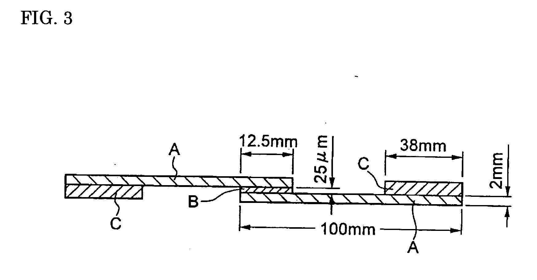
[0043] Composites having compositions shown in the Table given below were prepared to be used as base members of a member for a semiconductor device. More specifically, Cu—W or Cu—Mo composites were manufactured to have a substantially 100% concentration by using an infiltration method. An Al—SiC composite was manufactured by using a sintering method. In addition, a Si—SiC composite was manufactured by the infiltration method.

[0044] These composites are machined in the shape of plates having a dimension of 100 mm (length)×25 mm (width)×2 mm (height). The surfaces of the plates were subjected to grinding or blasting, so these composites have the values shown in the Table in a range of a surface roughness of 0.5 to 100 μm in Rmax. The samples 1 to 17 of the present invention were obtained by forming a coating layer made of a hard carbon (DLC) film having a thickness shown in the Table on the surface of each of the base members using a plasma CVD method. In addition, as comparative ex...


PUM

PropertyMeasurementUnit
thicknessaaaaaaaaaa
surface roughnessaaaaaaaaaa
depthaaaaaaaaaa

Abstract

There is provided a member for a semiconductor device, such as a substrate, having an excellent resin bonding property capable of improving resin bonding strength at the time the member for a semiconductor device being bonded with resin and maintaining a high resin bonding strength even after various reliability tests, such as a thermal cycling test, are performed. The member for a semiconductor device comprises a base member 1 made of an alloy or composite mainly composed of Cu and W and/or Mo, an alloy or composite mainly composed of Al—SiC, or an alloy or composite mainly composed of Si—SiC. A coating layer made of a hard carbon film 2 is provided on at least a surface of the base member 1 on which at least another member for the semiconductor device, such as a package, is bonded with a resin. It is preferable that the base member 1 have a surface roughness of 0.1 to 20 μm in Rmax. It is preferable that the hard carbon film 2 have a thickness of 0.1 to 10 μm.

Description

TECHNICAL FIELD [0001] The present invention relates to a member used for a heat sink, a radiating substrate, a housing, or the like constituting a semiconductor device, and more particularly, a member for a semiconductor device having an excellent resin bonding property and a semiconductor device using the same. BACKGROUND ART [0002] When a material constituting a substrate, which is one of the members for a semiconductor device, is combined with a member for another device, it is necessary that distortion due to thermal stress does not occur in the interface between the combined members. For this reason, the thermal expansion coefficient of the substrate material must not be largely different from those of other members for the semiconductor device, such as semiconductor elements or packages. In particular, as the semiconductor device has recently been made small and lightweight, the radiating substrate is required to be made of a material of a high thermal conductivity, the therm...

Claims


Application Information

Patent Timeline
Patent Type & Authority Applications(United States)
IPC IPC(8): H01L23/02H01L23/04H01L23/06H01L23/373
CPCH01L23/04H01L23/06H01L23/3732H01L2224/16H01L2224/73253H01L2924/01078H01L2924/01079H01L2924/01019H01L2924/15311H01L2924/16152H01L2224/16225H01L23/373H01L23/36
Inventor KAMITAKE, KAZUYAABE, YUGAKUHIGAKI, KENJIRO
Owner SUMITOMO ELECTRIC IND LTD
Why Eureka
Try Eureka