Semiconductor light emitting device, method for producing the same and reflector for semiconductor light emitting device

Inactive Publication Date: 2006-05-18
SANKEN ELECTRIC CO LTD
View PDF7 Cites 176 Cited by
  • Summary
  • Abstract
  • Description
  • Claims
  • Application Information

AI Technical Summary

Benefits of technology

[0017] The method for producing a semiconductor light emitting device according to the present invention comprises the steps of providing an assembly (10) which includes a metallic support plate (1) and a light-reflective reflector (3) attached on the support plate (1); mounting a semiconductor light emitting element (2) on the support plate (1); electrically connecting the light emitting element (2) to wiring conductor (5); setting the support plate (1) and reflector (3) in a cavity (23) of a forming mold (20) and clamping the support plate (12) and reflector (3) between upper and lower mold halves (21, 22) of the forming mold (20); and supplying a liquid resin into the cavity (23) of the forming mold (20) to form a plastic encapsulant (6). As the support plate (12) and reflector (3) are clamped between upper and lower mold halves (21, 22) of the forming mold (20), liquid resin is prevented from entering the interior of the reflector (3) to facilitate the molding operation.
[0018] The semiconductor light emitting device according to the present invention, comprises a support plate (1); a light-reflective reflector (3) mounted on the support plate (1) and formed with a hole (3a) upwardly diverging; and a semiconductor light emitting element (2) mounted on the support plate (1) within the hole (3a) of the reflector (3). The reflector (3) has a ledge (3d) connected to a wiring conductor (5) to electrically connect the light emitting element (2) and wiring conductor (5) through the ledge (3d) for easy and shortened wiring and improvement in reliability of semiconductor light emitting device. Also, the ledge (3d) can be embedded and securely fixed in the plastic encapsulant (6) by a molding process. In addition, the reflecting surface (3c) can be formed with a smaller diameter and with an increased height to enhance the directivity and axial brightness of light from the light emitting device.
[0019] The reflector for semiconductor light emitting device according to the present invention is secured on the support plate (1) surrounding the semiconductor light emitting element (2) on the support plate (1) to reflect upwardly light from the light emitting element (2). The reflector comprises a reflector block (3b) formed with a hole (3a) for defining a reflecting surface (3c) with the upwardly enlarging inner diameter and a notch (3k) formed on the reflector block (3b) between the hole (3a) and an outer side wall (3m) or between the light emitting element (2) and wiring conductor (5). A lead wire (8) passes through the notch (3k) to electrically connect the light emitting element (2) and wiring conductor (5) by substantially straight extending le

Problems solved by technology

To this end, new high power light emitting semiconductors have already been developed to produce a high intensity light when relatively large electric current for example more than 350 mA is supplied to the light emitting semiconductors, however, they have caused the following various problems.
Specifically, when the element is activated with a large electric current over 350 mA, it is heated so that a surface of semiconductor may reach a temperature above 150° C., and therefore, plastic encapsulant is also inconveniently awfully heated by heat from the semiconductor.
Such a resin tends to deteriorate under heat because it contains less additi

Method used


Image

  • Semiconductor light emitting device, method for producing the same and reflector for semiconductor light emitting device
  • Semiconductor light emitting device, method for producing the same and reflector for semiconductor light emitting device
  • Semiconductor light emitting device, method for producing the same and reflector for semiconductor light emitting device

Examples


Embodiment Construction

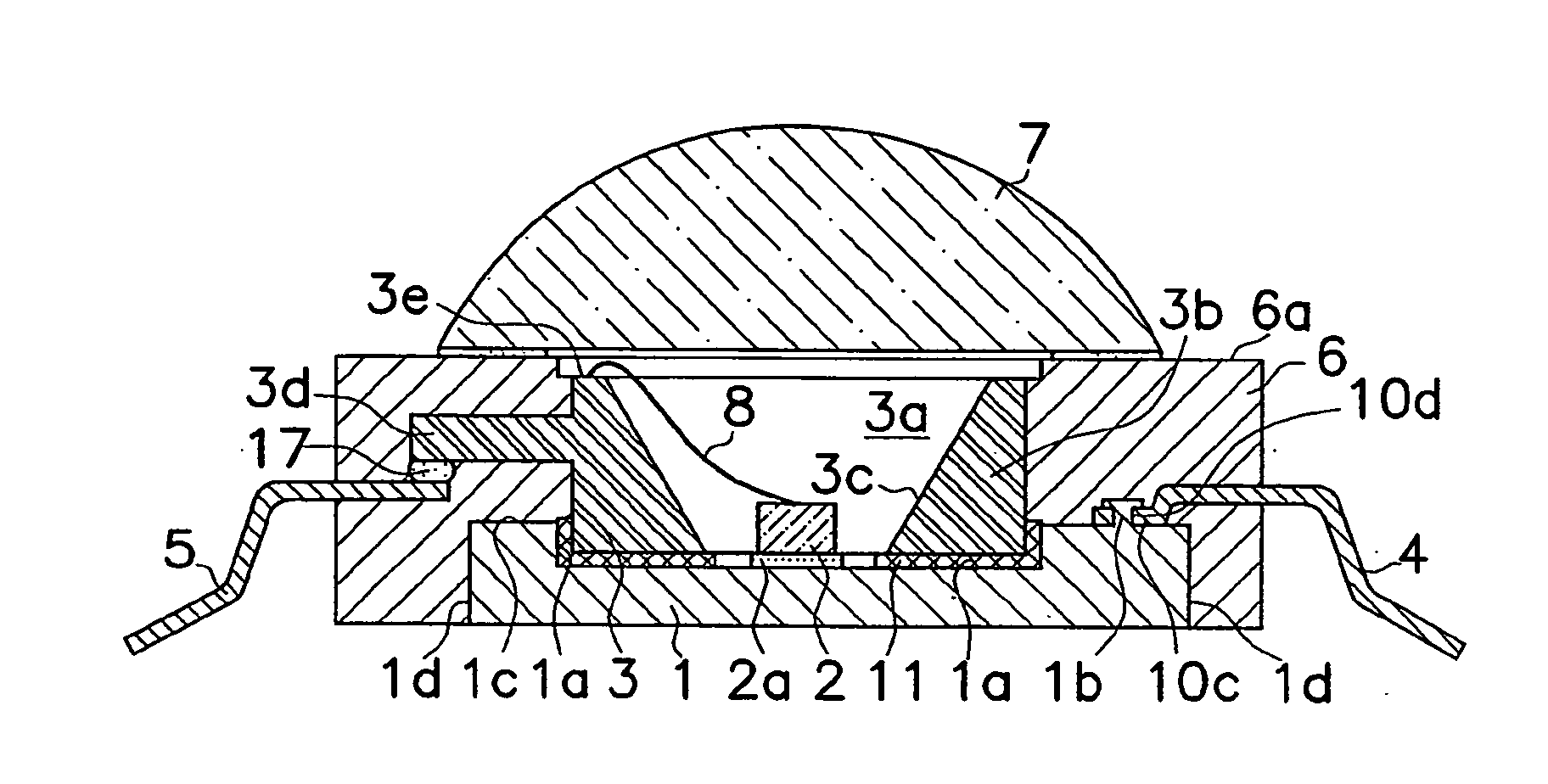
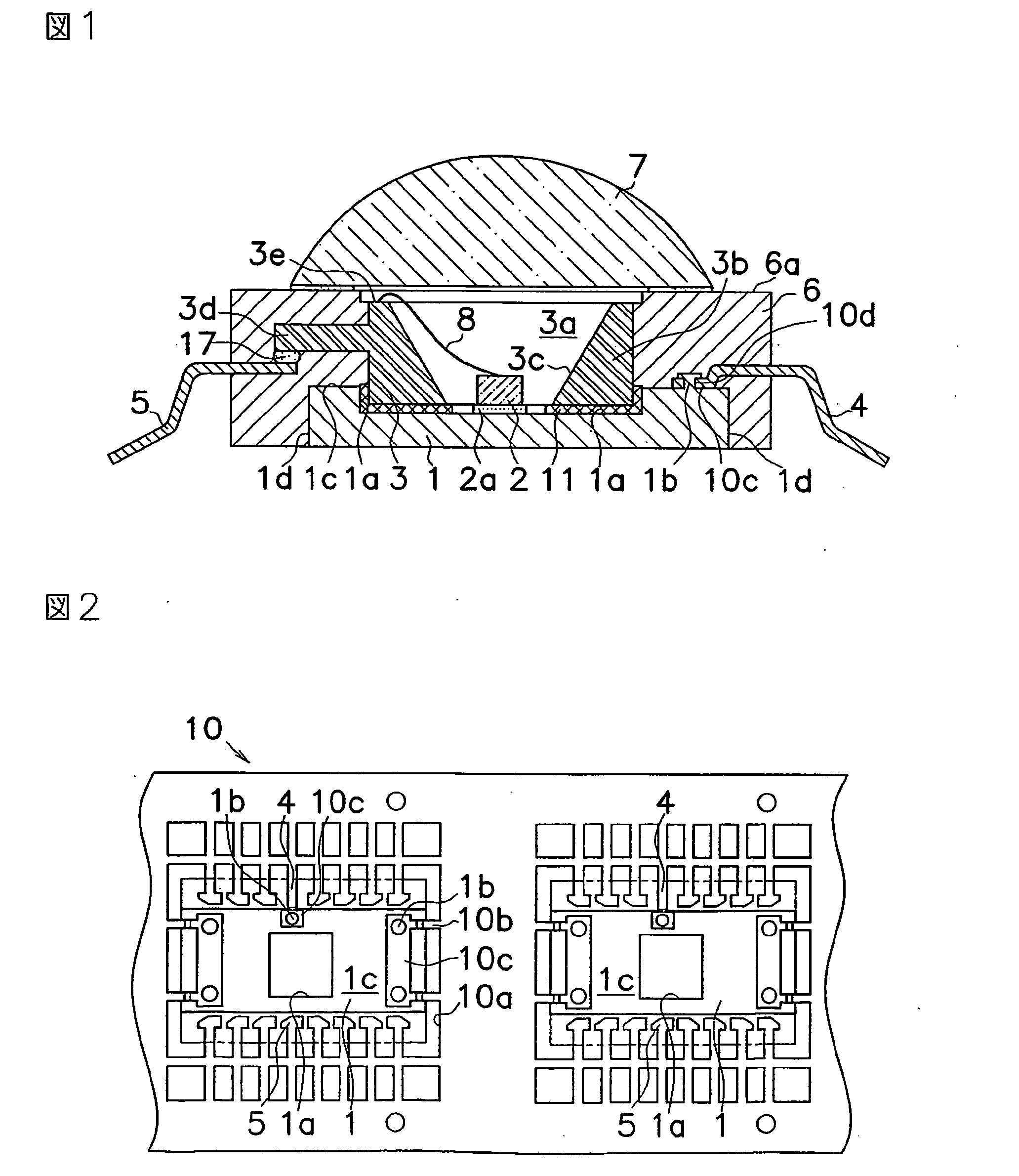
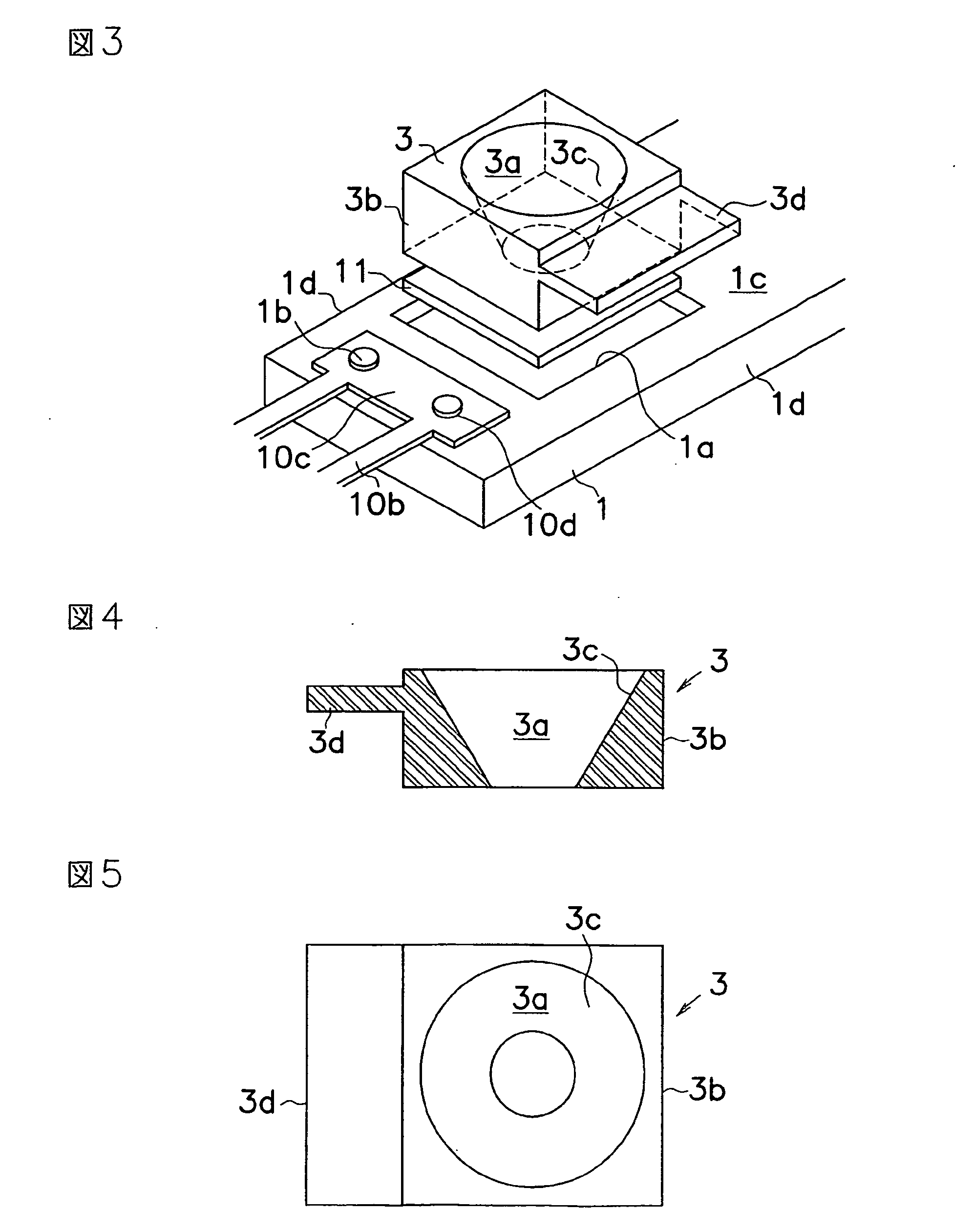
[0059] A semiconductor light emitting device shown in FIG. 1 comprises a metallic support plate 1 formed with a recess 1a; a light-reflective reflector 3 mounted in recess 1a of support plate 1 in electrically insulating relation to support plate 1, and formed with a hole 3a upwardly expanding; a light emitting diode 2 mounted on recess 1a of support plate 1 within hole 3a of reflector 3, one electrode (a bottom electrode) of the light emitting diode 2 being electrically connected to support plate 1; a first wiring conductor 4 electrically connected to support plate 1; a second wiring conductor 5 electrically connected to the other electrode (a top electrode) of light emitting diode 2; a lead wire 8 for electrically connecting light emitting diode 2 and reflector 3; a heat-resistible plastic encapsulant 6 for encapsulating outer periphery of reflector 3, upper and side surfaces 1c, 1d of support plate 1, each inner end of first and second wiring conductors 4, 5; and a lens 7 for cov...


PUM


Abstract

A semiconductor light emitting device comprises a metallic support plate 1; a light-reflective reflector 3 mounted on the support plate 1 and formed with a hole 3a; a semiconductor light emitting element 2 mounted on the support plate 1 within the hole 3a of the reflector 3, and a plastic encapsulant 6 for sealing an outer periphery of the reflector 3 and an upper surface 1c of the support plate 1. As the reflector 3 is electrically connected to a wiring conductor 5 or a lead wire 8 extends through a notch 3k formed in the reflector 3 to electrically connect the semiconductor light emitting element 2 and wiring conductor 5, wiring span of the lead wire 8 can be shortened to prevent deformation of the lead wire 8. Simultaneously, diameter of the reflective surface 3c in the reflector 3 is reduced and height of the reflector 3 is increased to improve directivity and axial brightness of light from the semiconductor light emitting device. Also, formation of the hole 3a effectively prevents further thermal degradation of heat-resistible plastic encapsulant 6 or other resin components.

Description

TECHNICAL FIELD [0001] This invention relates to a semiconductor light emitting device and a reflector for such a semiconductor light emitting device, in particular a semiconductor light emitting device, a method for producing the same and a reflector for the semiconductor light emitting device capable of avoiding harmful effect by heat and deformation of a lead wire connected to a light emitting element when they may occur with heavy electric current through the light emitting device. BACKGROUND OF THE INVENTION [0002] Japanese Patent Disclosure No. 11-340517 discloses a semiconductor light emitting device which comprises an insulating substrate formed with wiring conductors, a semiconductor element attached on a main surface of the substrate, a reflector (a light reflecting plate) surrounding the semiconductor element on the substrate, and a light-transmittable plastic encapsulant for encapsulating the semiconductor element and reflector. FIG. 36 illustrates a known semiconductor ...

Claims


Application Information

Patent Timeline
IPC IPC(8): H01L33/00H01L33/58H01L33/60H01L33/62H01L33/64
CPCH01L33/486H01L33/60H01L33/62H01L33/642H01L33/647H01L2224/48091H01L2224/48247H01L2224/73265H01L2924/01057H01L2924/01078H01L2924/01079H01L2924/3025H01L2924/00014H01L2924/01019H01L2924/12041H01L2224/16245
Inventor OYAMA, TOSHIHIKOKOBAYASHI, NOBUOOSAWA, HIDEYUKIOGATA, TOSHIO
Owner SANKEN ELECTRIC CO LTD
Why Eureka
Try Eureka