Semiconductor Wafer, Semiconductor Device, And Method Of Manufacturing Semiconductor Device

a semiconductor device and semiconductor technology, applied in the direction of semiconductor devices, semiconductor/solid-state device details, electric discharge tubes, etc., can solve the problems of difficult to determine, the electron beam cannot reach the alignment mark, and the excess formed, so as to achieve the effect of higher precision

Inactive Publication Date: 2006-05-18
FUJITSU SEMICON LTD
View PDF3 Cites 24 Cited by
  • Summary
  • Abstract
  • Description
  • Claims
  • Application Information

AI Technical Summary

Benefits of technology

[0021] Alternatively, the chip region of a semiconductor substrate may be employed as the second region, and the region included in this chip region may be employed as the first region. If doing this way, the distance between each point inside the chip region and the first region will be shorter as compared with the case where the first region is present outside the chip region. The positional misalignment of the chip region can be therefore corrected with higher precision by scanning the mark formed in the first region with the electron beam.

Problems solved by technology

However, in the case where a film for devices, such as a conductive film for gate electrodes, is formed on the semiconductor substrate 1, the recess which is formed under this conductive film and which an electron beam does not reach cannot be used as the alignment mark.
For this reason, as shown in the lower view of FIG. 2, because the S / N ratio of the graph 9 which indicates the intensity of the reflected electron becomes smaller, it is difficult to determine where the opening 3a exists, and thereby the alignment between the semiconductor substrate 1 and the electron beam exposure apparatus will be difficult.
However, the formation of such a conductive film 3 having a thick thickness makes it impossible to form refined gate electrodes.

Method used


Image

  • Semiconductor Wafer, Semiconductor Device, And Method Of Manufacturing Semiconductor Device
  • Semiconductor Wafer, Semiconductor Device, And Method Of Manufacturing Semiconductor Device
  • Semiconductor Wafer, Semiconductor Device, And Method Of Manufacturing Semiconductor Device

Examples


first embodiment

(1) First Embodiment

[0040]FIG. 3 is a block diagram of an electron beam exposure apparatus used in this embodiment.

[0041] This exposure apparatus includes an overall control system 101, a digital control system 106, an analog circuit 110, a machinery system 120, and an electron optics system column 113, and carries out exposure to a silicon substrate 10 inside the electron optics system column 113.

[0042] The overall control system 101 includes a control workstation 102, a display device 103 attached to this workstation, a hard disk 104, and a memory 105, and transmits / receives data to / from a digital control system 106 and the machinery system 120 via a bus 121. Such data includes, for example, a deflection data D which is generated by the control workstation 102 and determines the amount of deflection of the electron beam, which will be described hereinafter. This deflection data D is generated by the control workstation 102 depending on the shape and the size of device patterns s...

second embodiment

(2) Second Embodiment

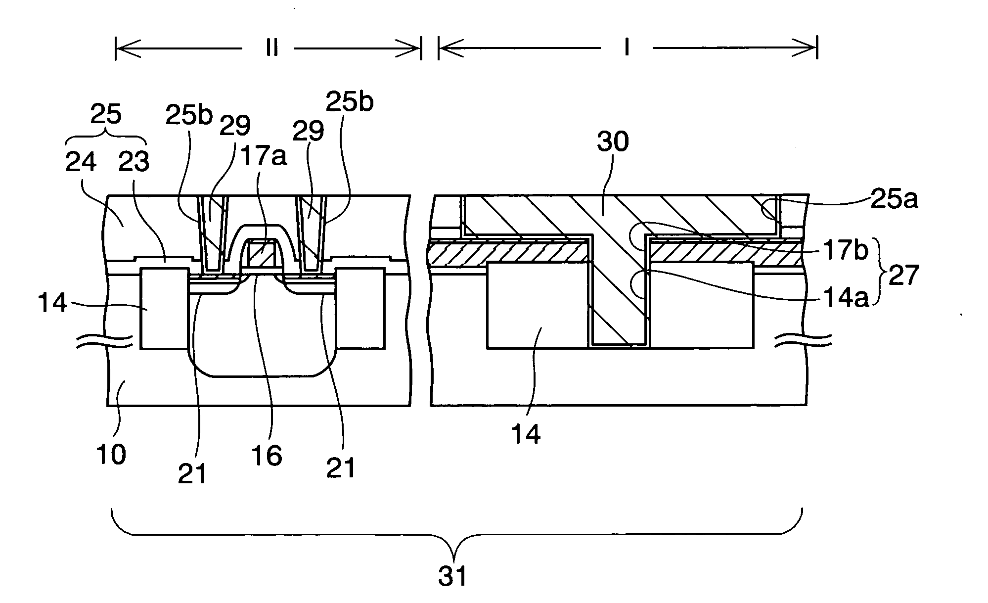
[0107] This embodiment differs only in the position of the first region I, in which the alignment mark 27 is formed, as compared with the first embodiment, and because the manufacturing method is the same as the first embodiment, the description regarding the manufacturing method is omitted.

[0108]FIG. 15 is a plan view of the semiconductor wafer according to this embodiment.

[0109] In the first embodiment described above, the first region I where the alignment mark 27 is formed is formed so as to be included in the scribe region. On the other hand, in this embodiment, as shown in FIG. 15, the first region is included in the chip region (the second region II).

[0110] With such an arrangement, the distance between the first region I and each point inside the chip region II becomes shorter as compared with the first embodiment in which the first region I exists outside the chip region II. It is therefore possible to correct the local positional misalignment for ea...


PUM


Abstract

Disclosed are a semiconductor wafer, a semiconductor device, and a method of manufacturing the semiconductor device, which are capable of easily carrying out an alignment between a semiconductor substrate and an electron beam exposure apparatus. There is provided a method including steps of: forming an interlayer insulating film 25 on a gate electrode 17a and a conductive film 17, as well as in a first opening 17b; forming in the interlayer insulating film 25 a second opening 25a including the first opening 17b; forming a hole 14a in an element isolation insulating film 14 under the first opening 17b; by use of the first opening 17b and the hole 14a as an alignment mark 27 used for the alignment in a state where a resist 28 is applied, measuring an intensity of a reflected electron EBref from the alignment mark 27, thus aligning the electron beam exposure apparatus with the semiconductor substrate 10; exposing with an electron beam EB the resist 28 existing in a hole formation region of a first region I; and developing the resist 28 to make a resist pattern 28e.

Description

CROSS-REFERENCE TO RELATED APPLICATIONS [0001] This application is based on and claims priority of Japanese Patent Application No. 2004-332345 filed on Nov. 16, 2004, the entire contents of which are incorporated herein by reference. BACKGROUND OF THE INVENTION [0002] 1. Field of the Invention [0003] The present invention relates to a semiconductor wafer, a semiconductor device, and a method of manufacturing the semiconductor device. [0004] 2. Description of the Related Art [0005] In order to manufacture a semiconductor device such as LSI, an exposure process for exposing photo resist is needed, but among many methods, an electron beam exposure which uses an electron beam is extremely effective for attaining the refining of semiconductor devices, because it has a high resolution characteristic. [0006] However, in order to fully bring out such a high resolution characteristic, it is necessary to carry out the alignment accurately between an electron beam exposure apparatus and a semi...

Claims


Application Information

Patent Timeline
Patent Type & Authority Applications(United States)
IPC IPC(8): H01L23/544
CPCH01J37/3045H01J2237/31754H01L23/544H01L2223/54426H01L2223/54453H01L2924/0002H01L2223/5446H01L2223/5448H01L2924/00
Inventor MARUYAMA, TAKASHI
Owner FUJITSU SEMICON LTD
Why Eureka
Try Eureka