Smart verify for multi-state memories

Inactive Publication Date: 2006-05-18
WODEN TECH INC
View PDF14 Cites 84 Cited by
  • Summary
  • Abstract
  • Description
  • Claims
  • Application Information

AI Technical Summary

Benefits of technology

[0019] According to one principal aspect of the present invention, briefly and generally, multi-state memories are programmed using a “smart verify” technique with a verify-results-based dynamic adjustment of the multi-states verify range for sequential-state-based verify implementations. The “smart verify” technique can increase multi-state write speed while maintaining reliable operation within sequentially verified, multi-state memory implementations. It does so by providing “intelligent” means to minimize the number of sequential verify operations for each p

Problems solved by technology

In practice, using this full verify set for each step in the programming is overkill and wastes time (wherein typically each verify sensing operation takes about the same time as a programming pulse), since at any point in the programming progression there will be only a limited Vth range (or range of data states) over which the population of cells can span.
Although this reduces the number of reads between programming pulses significantly compared to checking all the non-ground states (for example, 7 reads in the 3-bit example), there are a number of problems with using such a dead reckoning reduced scan, sliding window approach for higher write speed, while maintaining sufficient guard-band to the scan window to insure reliable write operation.
These problems mainly relate to the determination of sufficient guard-band.
In the case of inadequate verify span window, cells at both ends of the Vth distribution (i.e. both those which program too slowly or too quickly) may be missed when they in fact do achieve their proper Vth levels and require the programming lockout.
This will inevitably lead to co

Method used


Image

  • Smart verify for multi-state memories
  • Smart verify for multi-state memories
  • Smart verify for multi-state memories

Examples


Embodiment Construction

[0036] The various aspects of the present invention are applicable to non-volatile memory systems in general. Although the description below, as well as that in the Background, is given mainly in terms of an EEPROM Flash memory embodiment, the particular type of storage unit used in the memory array is not a limitation to the present invention. The particulars of how the storage elements are read, are written, and store data do not enter in to the main aspects of the present invention and can be those of any of the various non-volatile and volatile systems which likewise us sequential verification through state conditions to perform the cell by cell verify / program terminate operation.

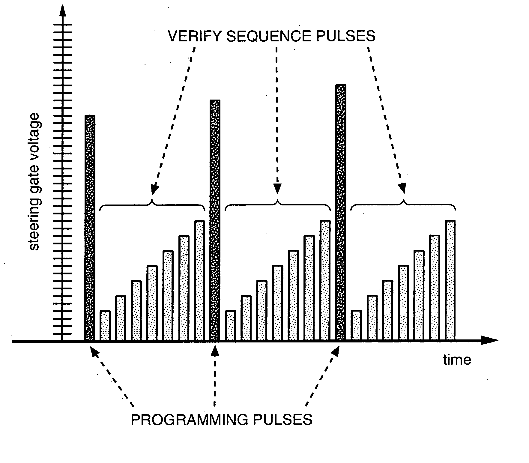
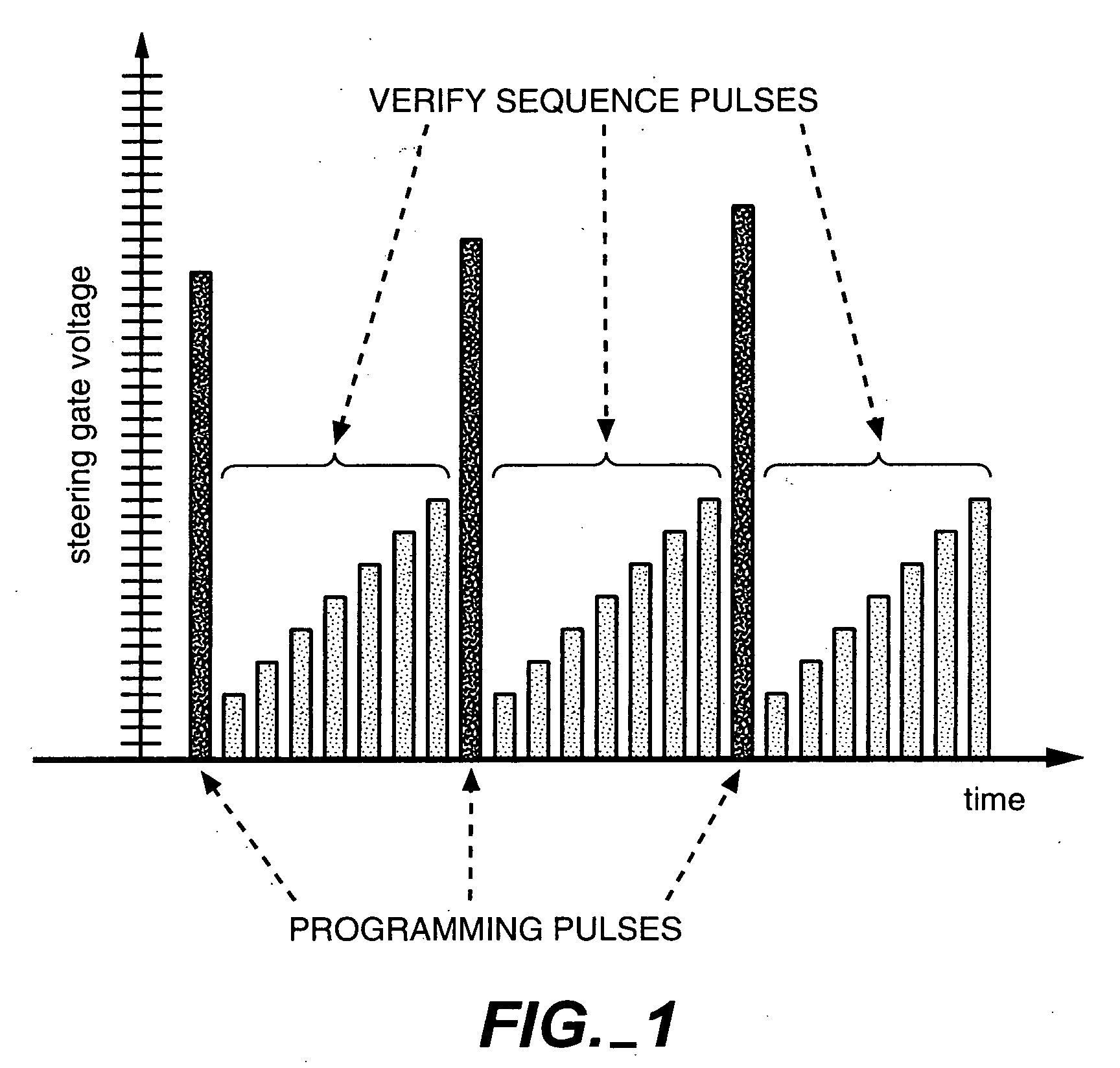
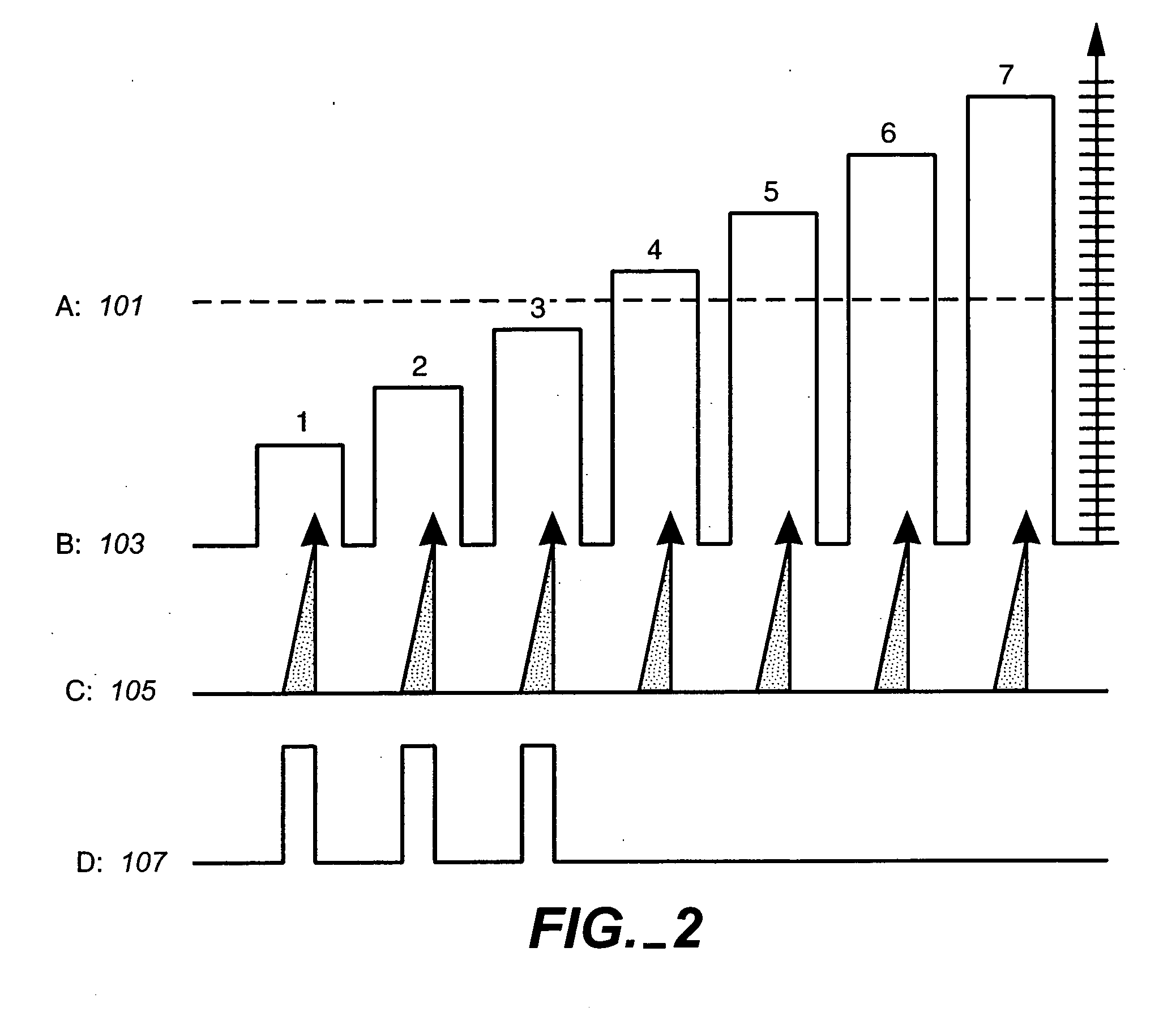
[0037] According to a principal aspect, the present invention uses verify-results-based dynamic adjustment of the multi-states verify range to establish a reliable, minimal time wasting multi-state write operation in sequential verification implementation. This provides a higher speed verify algorithm ...


PUM


Abstract

The present invention presents a “smart verify” technique whereby multi-state memories are programmed using a verify-results-based dynamic adjustment of the multi-states verify range for sequential-state-based verify implementations. This technique can increase multi-state write speed while maintaining reliable operation within sequentially verified, multi-state memory implementations. It does so by providing “intelligent” means to minimize the number of sequential verify operations for each program/verify/lockout step of the write sequence. In an exemplary embodiment of the write sequence for the multi-state memory during a program/verify cycle sequence of the selected storage elements, at the beginning of the process only the lowest state of the multi-state range to which the selected storage elements are being programmed is checked during the verify phase. Once the first storage state is reached by one or more of the selected elements, the next state in the sequence of multi-states is added to the verify process. This next state can either be added immediately upon the fastest elements reaching this preceding state in the sequence or after a delay of several program cycles. The adding of states to the set being checked in the verify phase continues through the rest of the set of multi-states in sequence, until the highest state has been added. Additionally, lower states can be removed from the verify set as all of the selected storage elements bound for these levels verify successfully to those target values and are locked out from further programming.

Description

CROSS REFERENCE TO RELATED APPLICATIONS [0001] This application is a continuation of U.S. patent application Ser. No. 10 / 314,055, filed Dec. 15, 2002, which is incorporated herein by reference in its entirety for all purposes.BACKGROUND OF THE INVENTION [0002] This invention pertains to the field of semiconductor non-volatile data storage system architectures and their methods of operation, and, in particular, relates to program verify methods. [0003] A number of architectures are used for non-volatile memories. A NOR array of one design has its memory cells connected between adjacent bit (column) lines and control gates connected to word (row) lines. The individual cells contain either one floating gate transistor, with or without a select transistor formed in series with it, or two floating gate transistors separated by a single select transistor. Examples of such arrays and their use in storage systems are given in the following U.S. patents and pending applications of SanDisk Co...

Claims


Application Information

Patent Timeline
IPC IPC(8): G11C29/00G11C11/56G11C16/34
CPCG11C11/5628G11C11/5635G11C2211/5621G11C16/3459G11C16/3454G11C29/00
Inventor GONGWER, GEOFFREY S.GUTERMAN, DANIEL C.FONG, YUPIN KAWING
Owner WODEN TECH INC
Why Eureka
Try Eureka