Light emitting diode

a technology of light-emitting diodes and diodes, which is applied in the direction of diodes, electrical equipment, basic electric elements, etc., can solve the problems of poor light-emitting efficiency of light-emitting diodes, inconsistent gap between two electrodes, and unsatisfactory electrode design of conventional large-area light-emitting diodes, etc., to achieve easy connection and reduce crowding

Inactive Publication Date: 2006-06-01
CHUNGHWA PICTURE TUBES LTD
View PDF8 Cites 136 Cited by
  • Summary
  • Abstract
  • Description
  • Claims
  • Application Information

AI Technical Summary

Benefits of technology

[0012] As described above, the first electrode and the second electrode of the light emitting diode of the present invention are arranged in a manner to render current distribution substantially uniform and thereby reduce the crowding effect. Furthermore, the redistributing circuit all

Problems solved by technology

However, the arrangement of the electrode design of the conventional large area light emitting diode is not ideal; for example, gaps between two electrodes are not consistent.
This will cause a non-uniform current distribution in the light emitting diode while driving it, and the light emitting efficiency of the ligh

Method used


Image

  • Light emitting diode
  • Light emitting diode
  • Light emitting diode

Examples


first embodiment

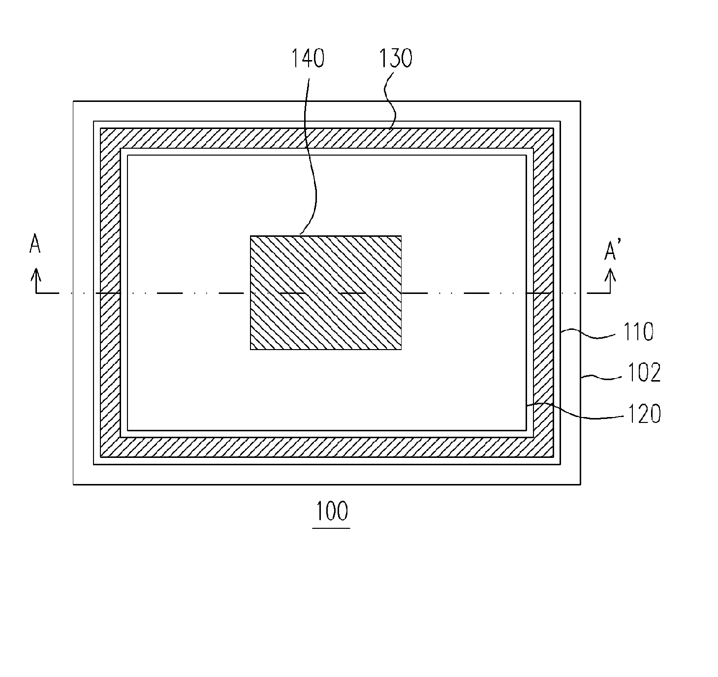
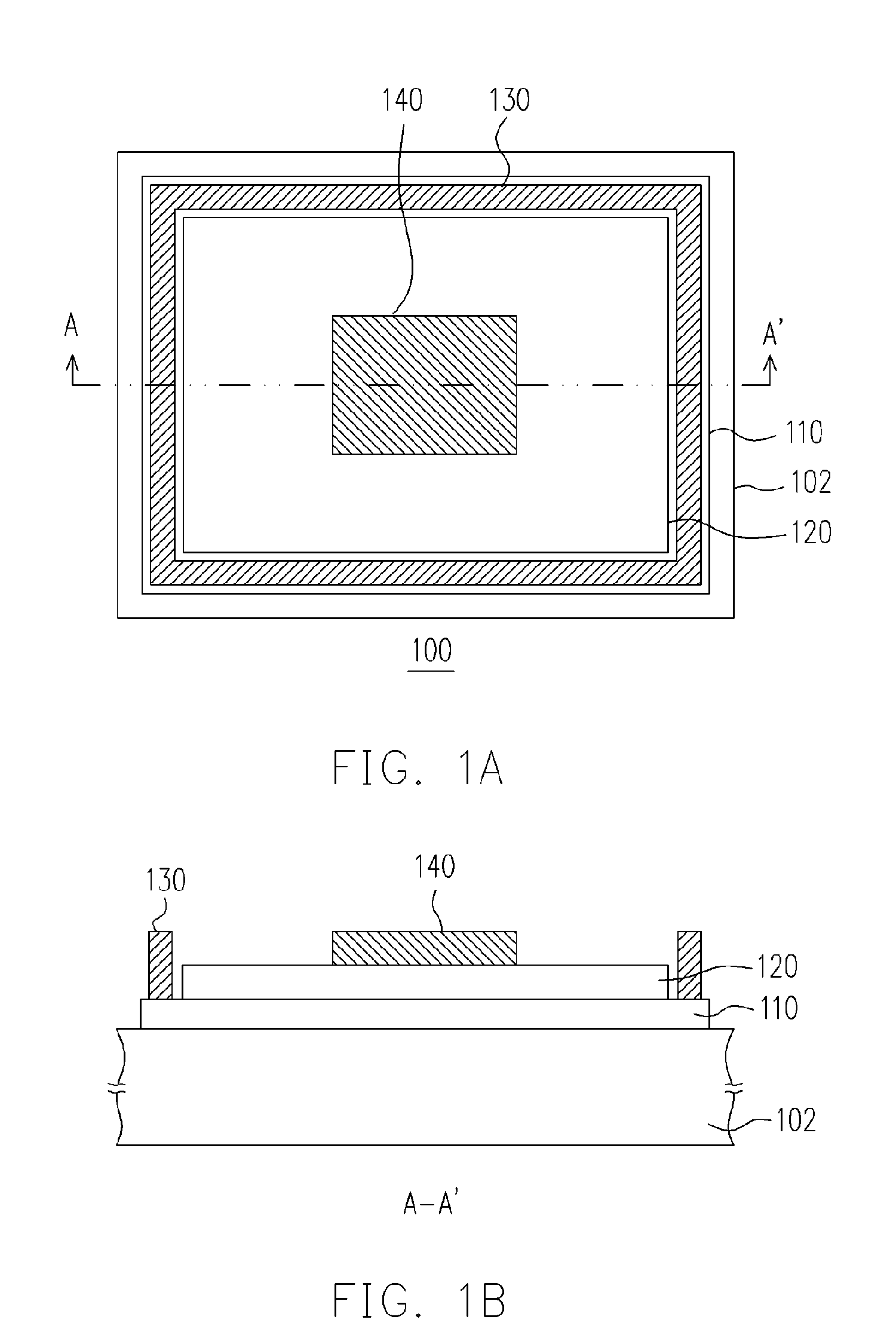
[0034]FIG. 1A is a schematic top view of a light emitting diode according to the first embodiment of the present invention, and FIG. 1B is a cross-sectional view of the light emitting diode along line A-A′ shown in FIG. 1A. The light emitting diode 100 comprises, for example but not limited to, a substrate 102, a first semiconductor layer 110 arranged on the substrate 102, and a second semiconductor 120 arranged on the first semiconductor layer 110. The second semiconductor layer 120 is disposed on the first semiconductor layer 110 such that a peripheral region of the first semiconductor layer 110 is exposed. The first semiconductor layer 110 and the second semiconductor layer 120 are respectively doped with dopants of different types. In one embodiment of the present invention, the first semiconductor layer 110 and the second semiconductor layer 120 are respectively doped with N-type dopant and P-type dopant; alternatively, the first semiconductor layer 110 and the second semicondu...

second embodiment

[0041]FIG. 4A is a schematic top view of a large area light emitting diode according to the second embodiment of the present invention, and FIG. 4B is a cross-sectional view of the large area light emitting diode along the line B-B′ shown in FIG. 4A. For example, a plurality of first semiconductor layers 210 is formed on a substrate 202 of a light emitting diode 200, and a second semiconductor layer 220 is disposed on each of the first semiconductor layers 210. In addition, a first electrode 230 and a second electrode 240 are respectively arranged on the first semiconductor layer 210 and the second semiconductor layer 220. Each first electrode 230 is disposed in a manner to surround the corresponding second electrode 240. In this manner, an array formed by a plurality of light emitting units 200a is constructed.

[0042]FIG. 5A is a schematic top view of the light emitting diode in FIG. 4A after the redistribution, and FIG. 5B is a cross-sectional view along line B-B′ in FIG. 5A. FIG....

third embodiment

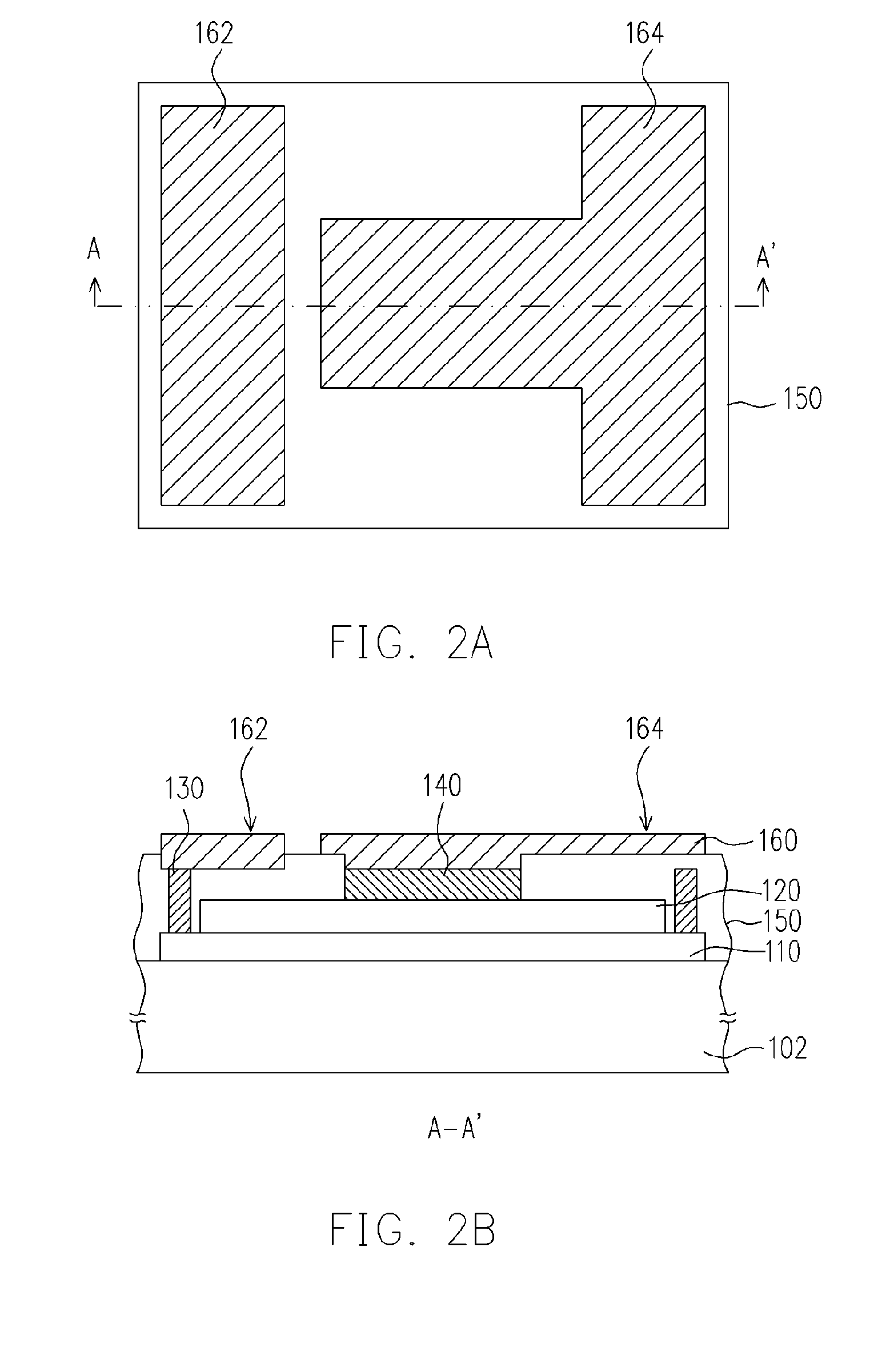
[0043]FIG. 7A is a schematic top view of a large area light emitting diode according to the third embodiment of the present invention, and FIG. 7B is a cross-sectional view of the large area light emitting diode along the line C-C′ shown in FIG. 7A. A plurality of light emitting units 300a is formed on a substrate 302 of a light emitting diode 300. The first electrode 330 of each light emitting unit 300a is arranged adjacent to each other, and each first electrode 330 surrounds its corresponding second electrode 340.

[0044] In addition, FIG. 8A is a schematic top view of the light emitting diode shown in FIG. 7A after the redistribution, and FIG. 8B is a cross-sectional view of the light emitting diode along line C-C′ shown in FIG. 8A. FIG. 9 shows a schematic circuit connection diagram of the light emitting units 300a. The first electrode 330 of each light emitting unit 300a is coupled to each other, and then coupled to the first extension electrode 362 through the redistributing c...


PUM


Abstract

A light emitting diode is provided, wherein a first semiconductor layer is disposed on a substrate, and a second semiconductor layer is disposed on the first semiconductor layer. The first and the second semiconductor layers are doped with different type dopants. In addition, a second electrode is disposed on the second semiconductor layer, and a first electrode is disposed on the first semiconductor layer to surround the second electrode. A dielectric layer is disposed on the substrate to isolates the first electrode from the second electrode. A redistributing circuit is disposed on the dielectric layer. The redistributing circuit is electrically connected to the first electrode and the second electrode to provide a first extending electrode and a second extending electrode. The light emitting diode can prevent the crowding effect and provide better reliability and light emitting efficiency.

Description

BACKGROUND OF THE INVENTION [0001] 1. Field of the Invention [0002] The present invention relates in general to a semiconductor device. More particularly, the present invention relates to a light emitting diode. [0003] 2. Description of Related Art [0004] The light emitting diode is a kind of semiconductor device. The major material of the light emitting chip comprises semiconductor compounds of III-V elements, such as gallium phosphide (GaP), gallium arsenide (GaAs), and gallium nitride (GaN), etc. The principle of a light emitting diode is to convert the electrical energy into light. In other words, when a current is applied to the semiconductor compound, electrons and holes in the semiconductor compound will annihilate to create energy, and this energy is released in the form of light so as to emit light. Since the light emitting diode is a kind of cold luminescence and not lit by heating or discharging, the lifetime of the light emitting diode can be up to about 100 thousand hou...

Claims


Application Information

Patent Timeline
IPC IPC(8): H01L33/00H01L33/08H01L33/38
CPCH01L27/156H01L33/08H01L33/38H01L2224/16245
Inventor CHEN, CHING-CHUNGWU, SHIN-MINYANG, CHING-ANLIN, WEI-CHIHLIU, MEI
Owner CHUNGHWA PICTURE TUBES LTD
Why Eureka
Try Eureka