Nonvolatile memory device and method including resistor and transistor

Inactive Publication Date: 2006-06-01
SAMSUNG ELECTRONICS CO LTD
View PDF19 Cites 26 Cited by
  • Summary
  • Abstract
  • Description
  • Claims
  • Application Information

AI Technical Summary

Benefits of technology

[0011] Example embodiments of the present invention provide a nonvolatile memory device having a resistor and a transistor, the

Problems solved by technology

However, after being turned off, data stored in DRAMs is lost.
Flash memory has a nonvolatile property, in contrast with volatile memory, but may have lower integration and/or may operate slower compared with DRAMs.
As described above, when a conventional

Method used


Image

  • Nonvolatile memory device and method including resistor and transistor
  • Nonvolatile memory device and method including resistor and transistor
  • Nonvolatile memory device and method including resistor and transistor

Examples


Example

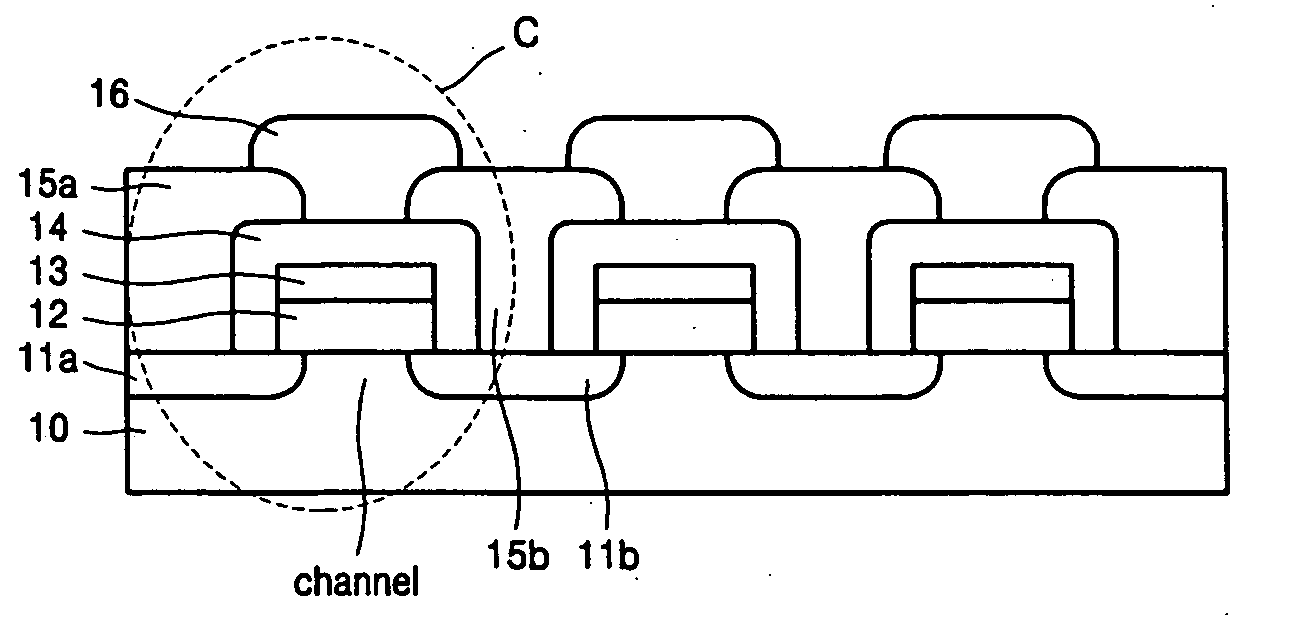
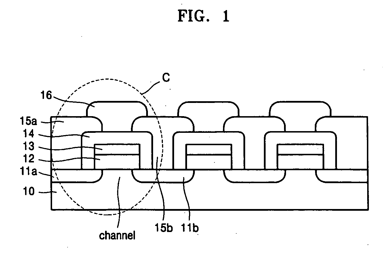
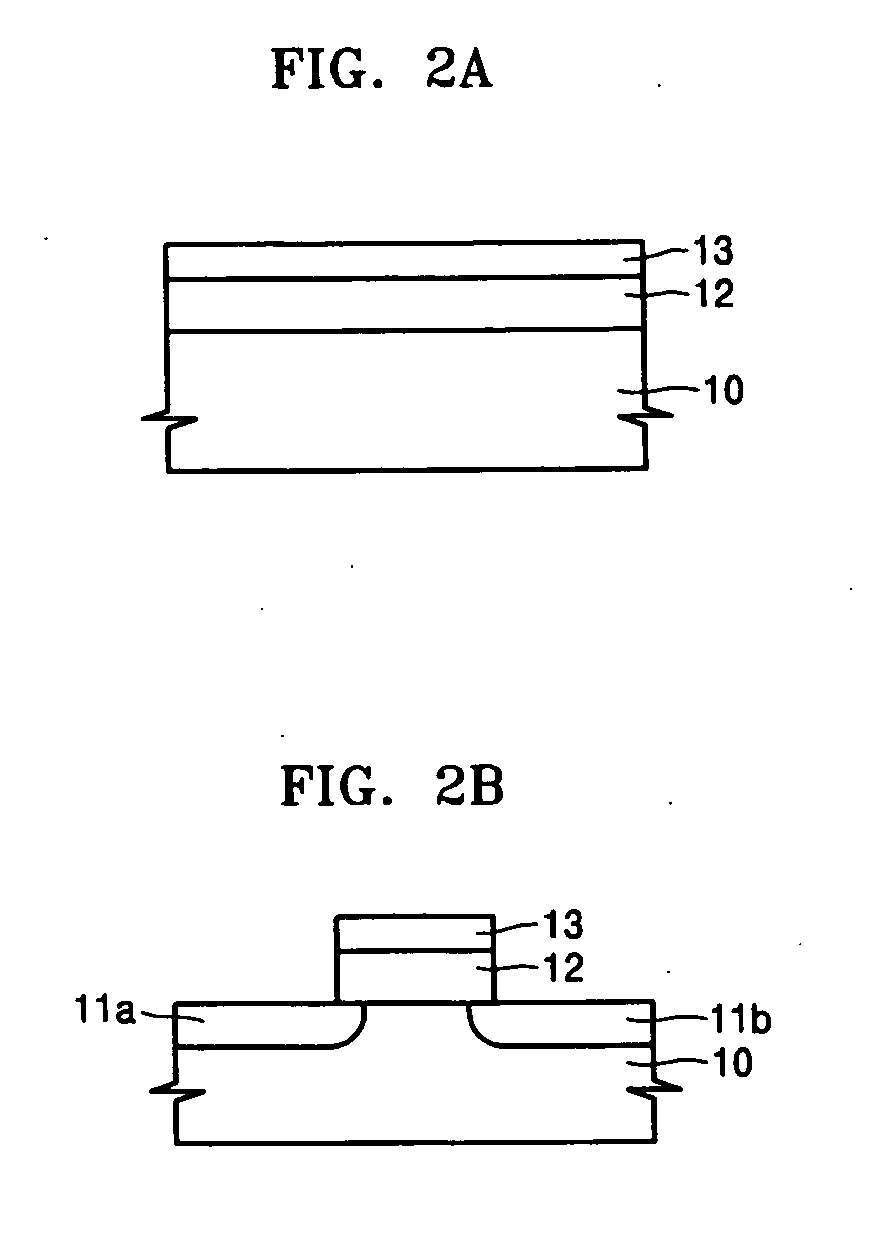
[0028] Example embodiments of the present invention will now be described in detail with reference to the accompanying drawings.

[0029] Various example embodiments of the present invention will now be described more fully with reference to the accompanying drawings in which some example embodiments of the invention are shown. In the drawings, the thicknesses of layers and regions are exaggerated for clarity.

[0030] Detailed illustrative embodiments of the present invention are disclosed herein. However, specific structural and functional details disclosed herein are merely representative for purposes of describing example embodiments of the present invention. This invention may, however, may be embodied in many alternate forms and should not be construed as limited to only the embodiments set forth herein.

[0031] Accordingly, while example embodiments of the invention are capable of various modifications and alternative forms, embodiments thereof are shown by way of example in the d...


PUM


Abstract

A nonvolatile memory device including one resistor and one transistor. The resistor may correspond to a resistance layer electrically connected to a first impurity region and a second impurity region of the transistor.

Description

PRIORITY STATEMENT [0001] This application claims the benefit of Korean Patent Application No. 10-2004-0090124, filed on Nov. 06, 2004, in the Korean Intellectual Property Office, the disclosure of which is incorporated herein in its entirety by reference. BACKGROUND OF THE INVENTION [0002] 1. Field of the Invention [0003] Example embodiments of the present invention relate to a nonvolatile memory device having one resistor and one transistor. [0004] 2. Description of the Related Art [0005] Semiconductor memory devices may have a high integration, that is, a large number of memory cells included per unit area, may operate at high speed, and may be driven at low power. Research into such semiconductor memory devices is ongoing and various types of memory devices are under development. [0006] Generally, a semiconductor memory device may include many memory cells connected together. In a dynamic random access memory (DRAM), which is a representative semiconductor memory device, a memor...

Claims


Application Information

Patent Timeline
IPC IPC(8): H01L29/94
CPCG11C13/0004G11C13/0007G11C13/003G11C2213/31G11C2213/32G11C2213/75H01L27/24H10B63/00H10N70/8828
Inventor YOO, IN-KYEONGLEE, MYOUNG-JAESEO, SUN-AESEO, DAVID
Owner SAMSUNG ELECTRONICS CO LTD
Why Eureka
Try Eureka