Solid-state imaging element and method of manufacturing the same

Active Publication Date: 2015-01-15
SMARTSENS TECH (SHANGHAI) CO LTD
View PDF1 Cites 4 Cited by
  • Summary
  • Abstract
  • Description
  • Claims
  • Application Information

AI Technical Summary

Benefits of technology

[0046]According to the solid-state imaging element and the method of manufacturing the same having the above characteristics, it becomes possible to incline the potential in the accumulation region, and accelerate the movement of the electric charges accumulated in the accumulation region to the transfer section only by adjusting the area per unit distance with respect to the transfer section or the density of the impurity concentration modulation regions formed in the accumulation region (the implantation region of the impurity having the first conductivity type or the second conductivity type in the accumulation region). Therefore, this solid-state imaging element can be simply ma

Problems solved by technology

However, when the accumulation region increases in size so that the solid-state imaging element is made highly sensiti

Method used


Image

  • Solid-state imaging element and method of manufacturing the same
  • Solid-state imaging element and method of manufacturing the same
  • Solid-state imaging element and method of manufacturing the same

Examples


first embodiment

First Example

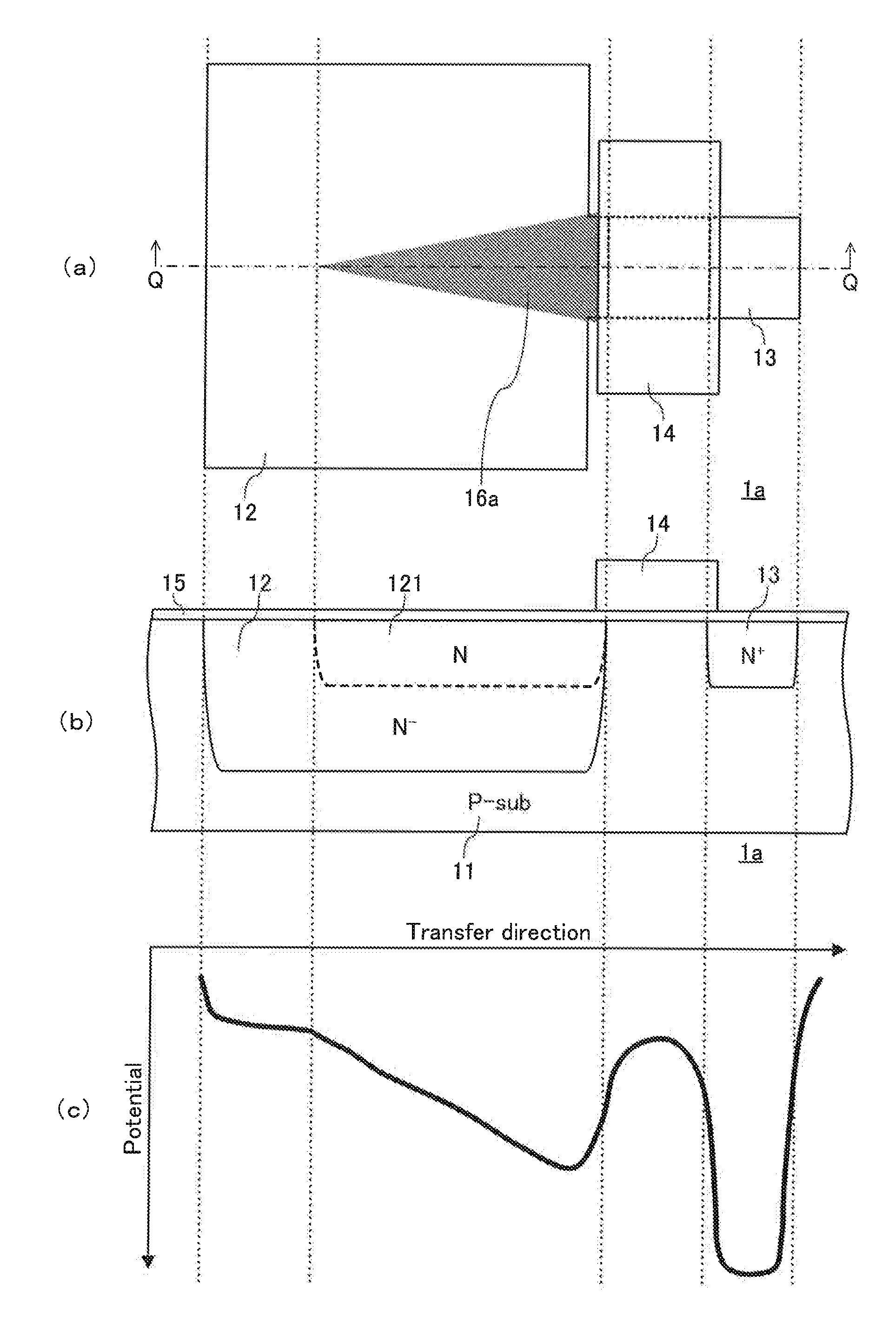
[0080]Hereinafter, solid-state imaging elements according to a first embodiment of the present invention will be described with reference to the drawings. First, a first example of the solid-state imaging element according to the first embodiment of the present invention will be described with reference to FIG. 3. FIG. 3 is a view showing the first example of the solid-state imaging element according to the first embodiment of the present invention. In addition, FIG. 3 (a) is a plan view of one pixel in the solid-state imaging element, FIG. 3 (b) is a cross-sectional view showing a cross-sectional surface taken along Q-Q in FIG. 3 (a). Furthermore, FIG. 3 (c) is a graph showing a potential in the cross-sectional surface taken along Q-Q in FIG. 3 (a).

[0081]As shown in FIGS. 3 (a) and (b), a solid-state imaging element 1a includes a substrate 11, an accumulation region 12 formed in the substrate 11, for accumulating electrons generated in the substrate 11 by a photoelectr...

second embodiment

First Example

[0123]Hereinafter, solid-state imaging elements according to a second embodiment of the present invention will be described with reference to the drawings. First, a first example of the solid-state imaging element according to the second embodiment of the present invention will be described with reference to FIG. 12. FIG. 12 is a view showing the first example of the solid-state imaging element according to the second embodiment of the present invention. In addition, FIG. 12 (a) is a plan view of one pixel in the solid-state imaging element, FIG. 12 (b) is a cross-sectional view showing a cross-sectional surface taken along R-R in FIG. 12 (a). Furthermore, FIG. 12 (c) is a graph showing a potential in the cross-sectional surface taken along R-R in FIG. 12 (a).

[0124]As shown in FIG. 12 (a) (b), a solid-state imaging element 2a includes a substrate 21, an accumulation region 22 formed in the substrate 21, for accumulating electrons generated by a photoelectric conversion,...

second example

[0130]Next, a second example of the solid-state imaging element according to the second embodiment of the present invention will be described with reference to FIG. 13. FIG. 13 is a view showing the second example of the solid-state imaging element according to the second embodiment of the present invention. In addition, FIG. 13 corresponds to FIG. 12 (a) showing the first example of the solid-state imaging element according to the second embodiment of the present invention. Furthermore, the present example differs from the first example only in an implantation region and a non-implantation region, and the present and the first examples are the same other than that. Therefore, hereinafter, only a non-implantation region 261b and an implantation region 262b in the present example will be described, and as for the rest of it, the description in the first example of the second embodiment described above and FIG. 12 is to be occasionally used as references, and its description is omitte...


PUM


Abstract

Provided are a solid-state imaging element which can be simply manufactured and can control movement of electric charges in an accumulation region with a high degree of accuracy, and a method of manufacturing the same. A solid-state imaging element (1a) includes a substrate (11) having a first conductivity type; an accumulation region (12) having a second conductivity type and provided in the substrate (11); a read-out region (13) for receiving the transferred electric charges accumulated in the accumulation region (12); and a transfer section (14) for transferring the electric charges from the accumulation region (12) to the read-out region (13). An impurity concentration modulation region 121 having a locally high concentration of an impurity having the second conductivity type, or having a locally low concentration of an impurity having the first conductivity type is formed in a part of the accumulation region (12). An area of the impurity concentration modulation region (121) per unit distance with respect to the transfer section (14), or a density of the discretely provided impurity concentration modulation region (121) increases with decreasing distance to the transfer section (14).

Description

TECHNICAL FIELD[0001]The present invention relates to a solid-state imaging element typified by a CMOS (Complementary Metal Oxide Semiconductor) imaging sensor, a CCD (Charge Coupled Device) imaging sensor, or the like.BACKGROUND ART[0002]The solid-state imaging element such as the CCD imaging sensor or the CMOS imaging sensor is mounted on an imaging device such as a digital video camera or a digital still camera, and is mounted on various kinds of electronic devices each having an imaging function, such as a camera cell-phone, a scanner, a copying machine, and a fax machine.[0003]The solid-state imaging element includes a photoelectric conversion unit such as a photodiode in a substrate to generate electric charges by photoelectrically converting light inputted to the substrate. The generated electric charges are accumulated in an accumulation region in the substrate, and are subsequently transferred to a read-out region in the substrate through a transfer section. Thus, based on ...

Claims


Application Information

Patent Timeline
IPC IPC(8): H01L27/148H01L31/0352
CPCH01L31/03529H01L27/14812H01L27/1461H01L27/14616H01L27/14612
Inventor USHINAGA, TAKEO
Owner SMARTSENS TECH (SHANGHAI) CO LTD
Why Eureka
Try Eureka