Electron emission device, electron emission display apparatus having the same, and method of manufacturing the same

Inactive Publication Date: 2010-07-01
SAMSUNG SDI CO LTD
View PDF5 Cites 5 Cited by
  • Summary
  • Abstract
  • Description
  • Claims
  • Application Information

AI Technical Summary

Benefits of technology

[0016]The present invention provides an electron emission device that can uniformly emit electrons and can be simply manufactu

Problems solved by technology

A display apparatus that displays an image using a FEA type electron emission device often has non-uniform brightness between pixels which may occur due to variation in the voltages applied to re

Method used


Image

  • Electron emission device, electron emission display apparatus having the same, and method of manufacturing the same
  • Electron emission device, electron emission display apparatus having the same, and method of manufacturing the same
  • Electron emission device, electron emission display apparatus having the same, and method of manufacturing the same

Examples


Example

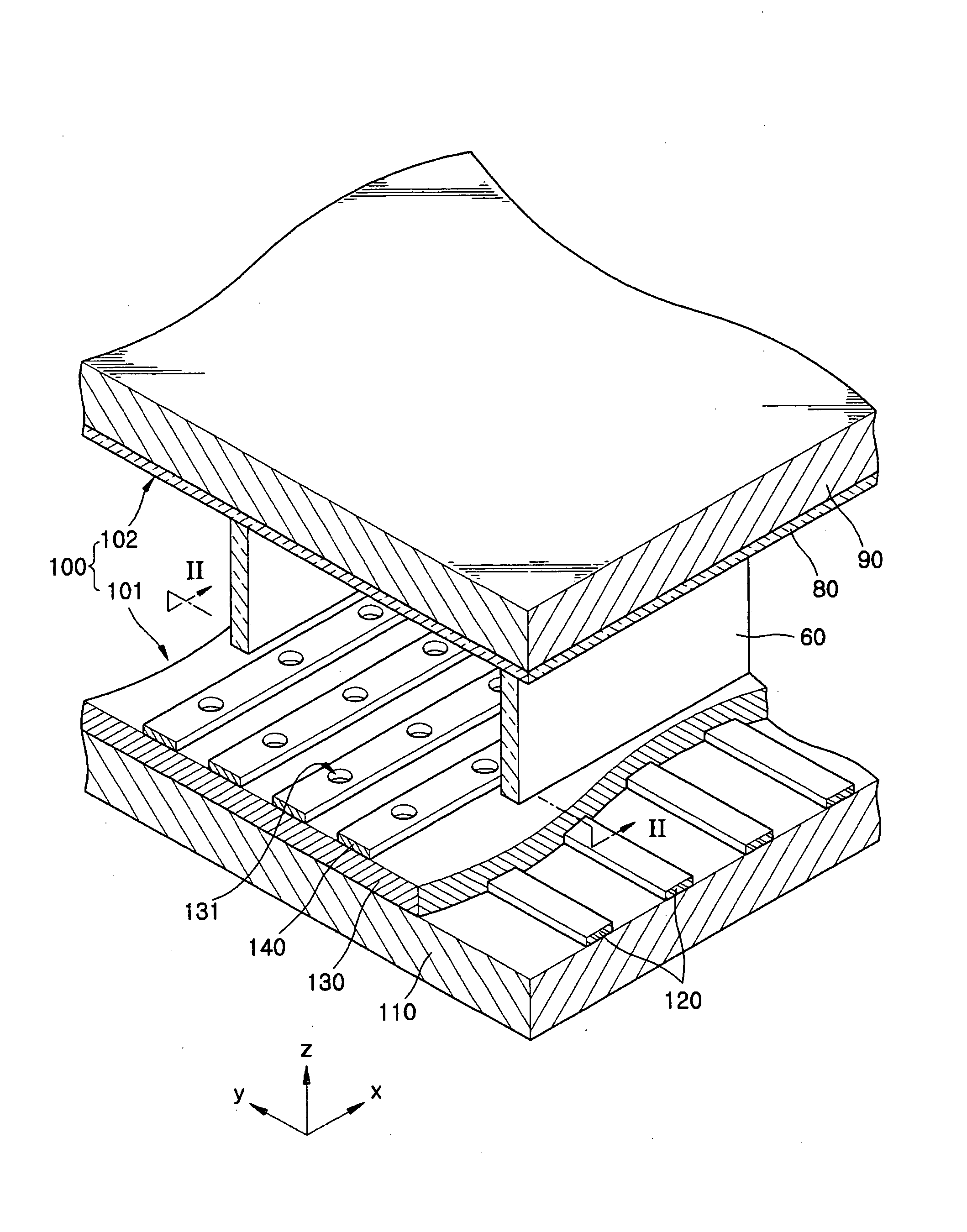
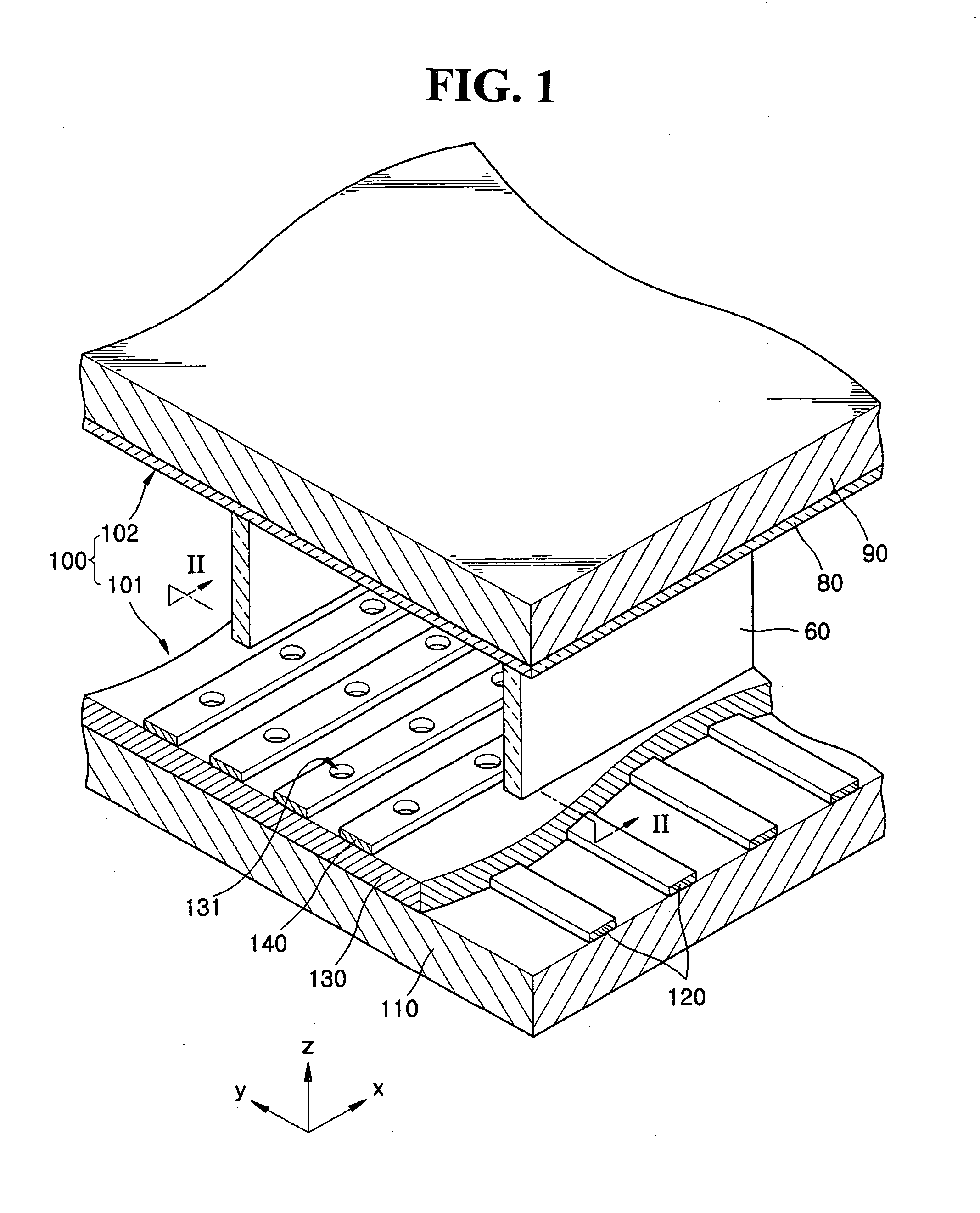
[0041]An example of a display apparatus that uses the field emitter array type electron emission device is depicted in FIGS. 1 and 2 for showing a general concept.

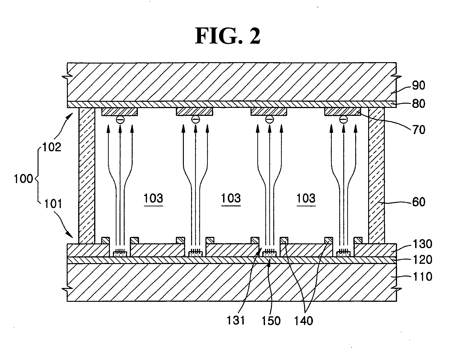
[0042]FIG. 1 is a partial perspective view of a top gate type electron emission display apparatus 100, and FIG. 2 is a cross-sectional view taken along line II-II of FIG. 1.

[0043]Referring to FIGS. 1 and 2, the electron emission display apparatus 100 includes an electron emission device 101 and a front panel 102, which are located parallel to each other and form a vacuum space 103, and a spacer 60 that maintains a gap between the electron emission device 101 and the front panel 102.

[0044]The electron emission device 101 includes a first substrate 110, a plurality of gate electrodes 140 and a plurality of cathodes 120 crossing the gate electrodes 140 on the first substrate 110, and an insulating layer 130 which is located between the gate electrodes 140 and the cathodes 120 and electrically insulates the gate electrodes 140...


PUM


Abstract

An electron emission device that can uniformly emit electrons and has low manufacturing costs, a display apparatus having improved pixel uniformity by using the electron emission device, and a method of manufacturing the electron emission device, wherein the electron emission device includes a first substrate, a cathode and an electron emission source disposed on the first substrate, a gate electrode electrically insulated from the cathode, an insulating layer interposed between the cathode and the gate electrode to insulate the cathode from the gate electrode, and a resistance layer that contacts the cathode and includes semiconductive carbon nanotubes (CNTs).

Description

CROSS-REFERENCE TO RELATED PATENT APPLICATION AND CLAIM OF PRIORITY[0001]This application claims the benefit of Korean Patent Application No. 10-2005-0093117, filed on Oct. 4, 2005, in the Korean Intellectual Property Office, the disclosure of which is incorporated herein in its entirety by reference.BACKGROUND OF THE INVENTION[0002]1. Field of the Invention[0003]The present invention relates to an electron emission device, an electron emission display apparatus that uses the electron emission device, and a method of manufacturing the same, and more particularly, to an electron emission device having a structure in which a voltage applied to an electron emission source is uniformly distributed, an electron emission display apparatus having the electron emission device to increase brightness uniformity of pixels, and a method of manufacturing the same.[0004]2. Description of the Related Art[0005]Generally, electron emission devices use a thermal cathode or a cold cathode as an electr...

Claims


Application Information

Patent Timeline
IPC IPC(8): H01J1/62H01J1/02H01J9/02
CPCH01J29/04H01J31/127C01B32/158B82Y40/00H01J1/30
Inventor CHOI, YOUNG-CHULPARK, JONG-HWANCHOE, DEOK-HYEON
Owner SAMSUNG SDI CO LTD
Why Eureka
Try Eureka