Current sensor

a current sensor and small technology, applied in the field of current sensors, can solve the problems of affecting the transmission of signal current as direct current, adverse influence on the communication system, and different load applied to the communication system, and achieve the effect of suppressing the whole resistance value, high sensitivity, and high precision

Active Publication Date: 2006-06-01
TDK CORPARATION
View PDF4 Cites 74 Cited by
  • Summary
  • Abstract
  • Description
  • Claims
  • Application Information

AI Technical Summary

Benefits of technology

[0011] In the current sensor of the invention, the first magnetoresistive element is disposed closer to the first thin film coil 31 in comparison with the case where the first magnetoresistive element and the first thin film coil are provided so as to be adjacent each other in the in-plane direction. Consequently, the whole dimension is reduced, and the first current magnetic field based on the current to be detected which flows in the first thin film coil is applied more strongly to the first magnetoresistive element. At this time, the first current magnetic field generated by the plurality of winding body portions of the first thin film coil corresponding to the plurality of element patterns of the first magnetoresistive element is applied to the plurality of element patterns. Therefore, optimization of the positions and dimensions in the cross section orthogonal to the first direction can be easily achieved from the viewpoint of heating by the coil and current efficiency of the coil magnetic field strength. As compared with the case of applying a current magnetic field generated only by a current flowing in one conductor (winding body portion) to each of the element patterns, the first current magnetic field can be effectively applied to each of the element patterns.
[0016] The current sensor of the invention has: a first magnetoresistive element including a plurality of strip-shaped element patterns which extend in a first direction at a first level and are disposed so as to be adjacent to each other in a second direction orthogonal to the first direction; and a first thin film coil which includes a plurality of winding body portions extending in the first direction in correspondence with the element patterns in the first magnetoresistive element, winds at a second level, and applies a first current magnetic field to each of the element patterns in the first magnetoresistive element when a current to be detected is supplied. Consequently, while having a compact configuration, the current to be detected flowing in the first thin film can be measured with high sensitivity and high precision. In this case, in particular, by connecting the element patterns in the first magnetoresistive element in parallel with each other, the whole resistance value can be suppressed to be relatively low without decreasing the resistance change ratio in the first magnetoresistive element, and the heat generation amount of the first magnetoresistive element at the time of use can be reduced. Moreover, the influence of noise from the outside (unnecessary magnetic fields) can be reduced, and the S / N ratio can be improved. On the other hand, when the element patterns in the first magnetoresistive element are connected in series to each other, the total length of the element patterns functioning as a magnetosensitive part can be increased without increasing the dimension in the first direction, and the absolute values of general resistance values (impedances) in the first magnetoresistive element can be further increased. Therefore, high-precision measurement can be performed even with a weaker current to be detected.
[0017] When the current sensor according to the invention further includes a second thin film coil which includes a plurality of winding body portions extending in the first direction in correspondence with the element patterns in the first magnetoresistive element and winds at a third level positioned on the side opposite to the second level with respect to the first level as a reference, and applies a second current magnetic field in the same direction as that of the first current magnetic field to each of the element patterns in the first magnetoresistive element when the current to be detected is supplied, a combined magnetic field of the first and second current magnetic fields is applied to each of the element patterns. Thus, the absolute value of the resistance change amount in the first magnetoresistive element can be further increased, and the current to be detected can be measure with higher precision.

Problems solved by technology

In this case, however, a load different from that in a communication system is applied, and there is the possibility that an adverse influence is exerted on the communication system.
Moreover, a frequency band in which the signal current as the direct current can be transmitted is limited.
At a frequency other than the proper frequency band, the impedance of the transformer changes, so that it lacks linearity, and an adverse influence may be exerted on the communication device and the like.
On the other hand, the photocoupler has excellent frequency characteristics but it is difficult to reduce the size when the photocoupler is used.
There is also a problem such that, thinking in long terms, deterioration in signal intensity caused by a change with time tends to occur.
In a conventional current sensor using conventional GMR elements, however, a GMR element is provided so as to be adjacent to a line to be measured in an in-plane direction, so that it is difficult to detect weak current and it is disadvantageous from the viewpoint of miniaturization.

Method used


Image

  • Current sensor
  • Current sensor
  • Current sensor

Examples


first embodiment

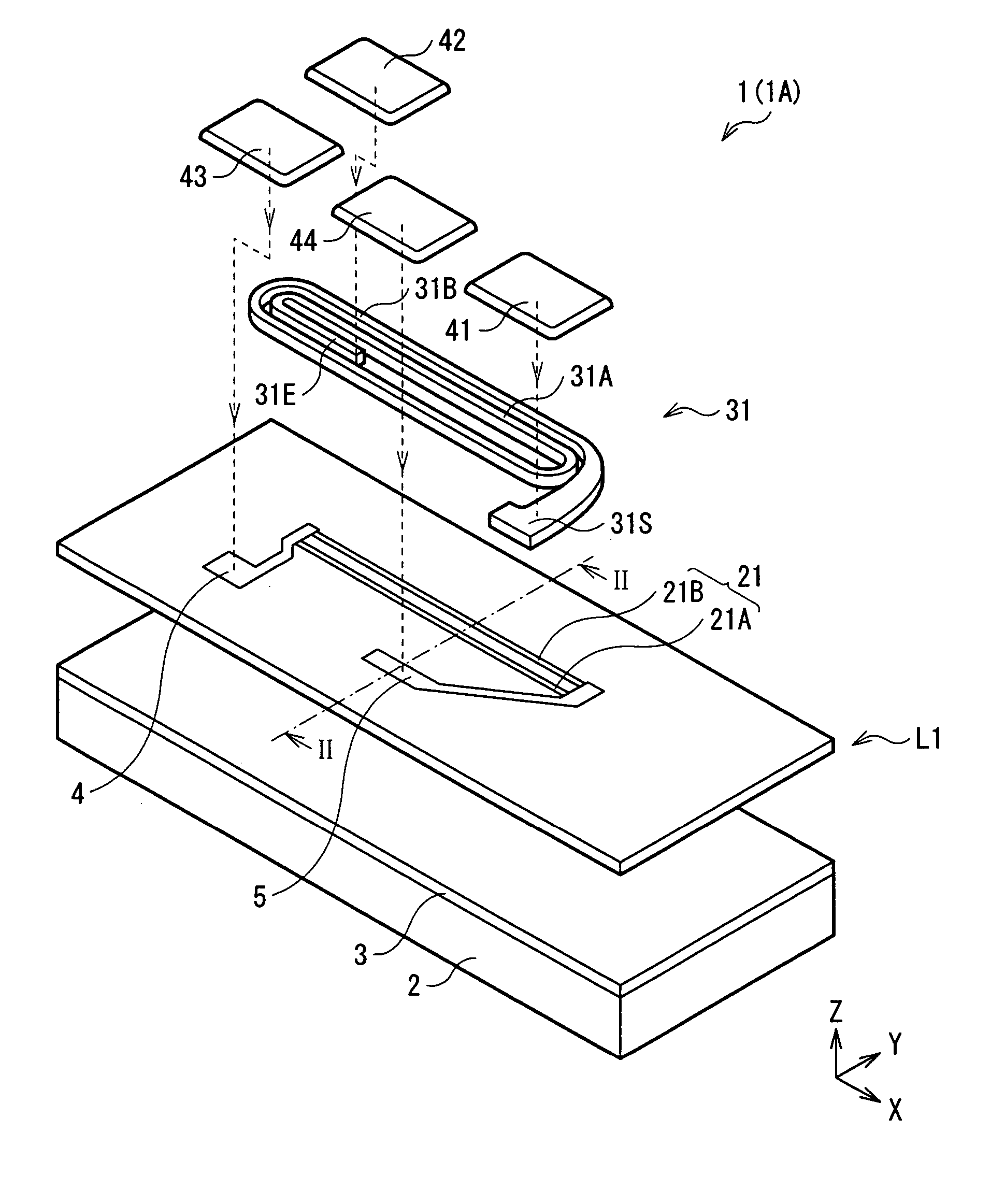
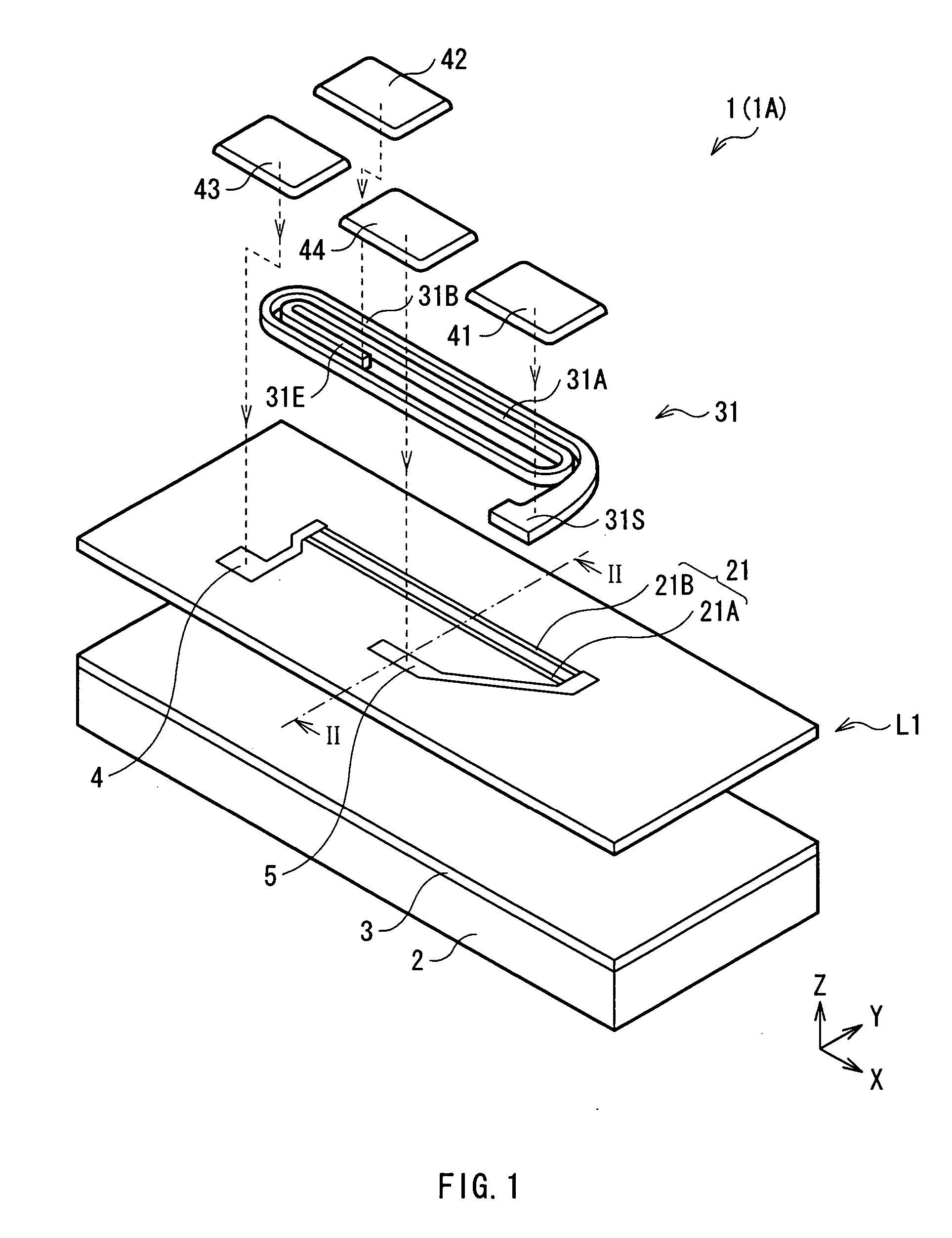
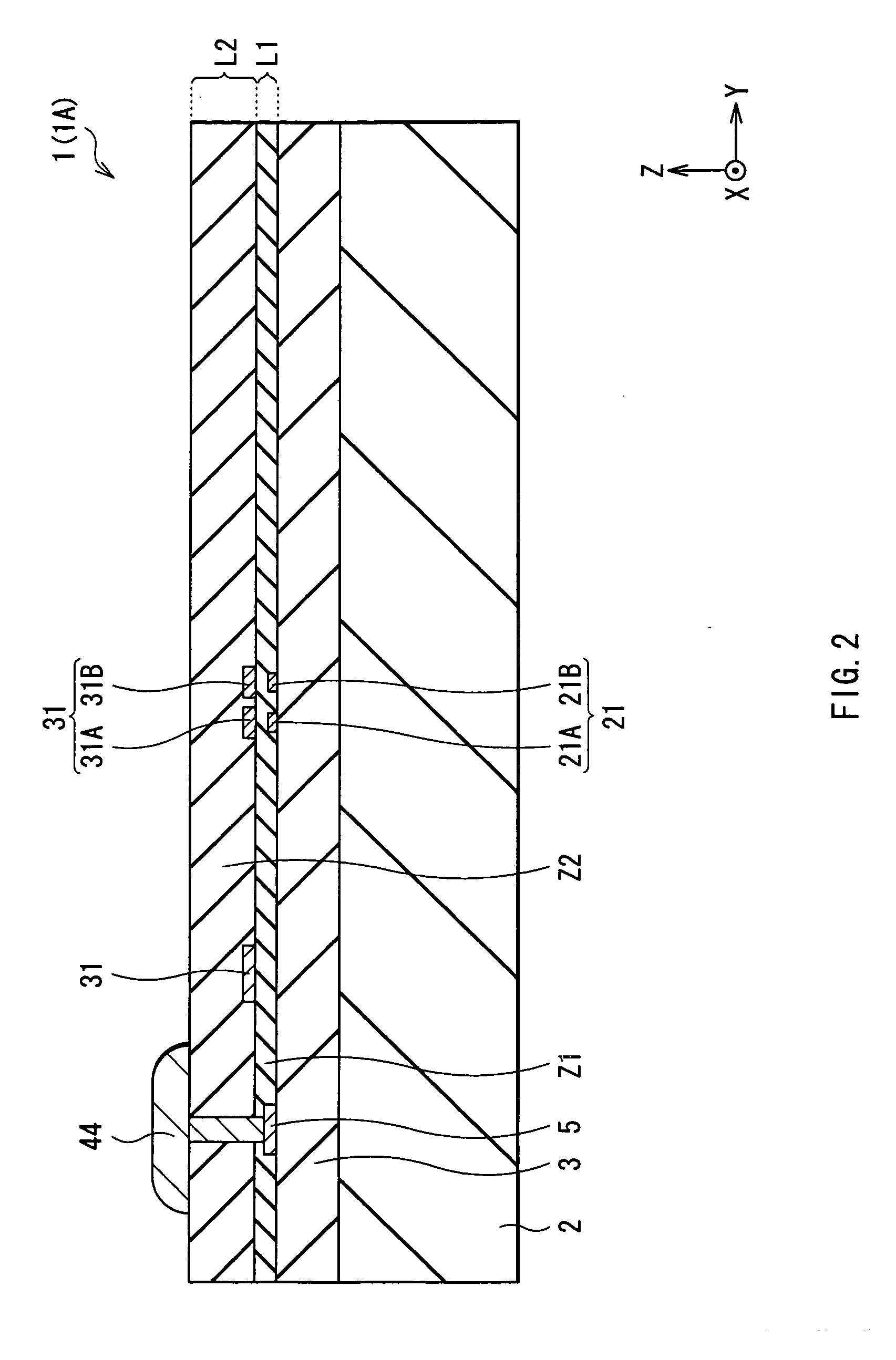
[0039] First, the configuration of a current sensor as a first embodiment of the invention will be described with reference to FIGS. 1 and 2. FIG. 1 is a schematic view illustrating a perspective configuration of a current sensor 1 according to the embodiment. FIG. 2 is a cross section taken along line II-II of the current sensor 1 illustrated in FIG. 1 seen from the direction indicated by the arrows (−X direction). The current sensor 1 is mounted on, for example, a communication device and is used for accurately measuring a current as a control signal. To distinguish the current sensor of the first embodiment from that of a second embodiment to be described later and the like, the current sensor in the first embodiment will be called a current sensor 1A.

[0040] The current sensor 1A includes a first magnetoresistive element 21 having two element patterns 21A and 21B extending in a first direction (X axis direction) at a first level L1, and a first thin film coil 31 (hereinbelow, si...

second embodiment

[0057] Subsequently, a current sensor 1B as a second embodiment of the invention will be described with reference to FIGS. 9 and 10.

[0058]FIG. 9 is schematic view illustrating a perspective configuration of the current sensor 1B. FIG. 10 shows a sectional configuration taken along line X-X of the current sensor 1B in FIG. 9 seen from the direction indicated by the arrows (−X direction). The current sensor 1B is obtained by adding a second thin film coil 32 (hereinbelow, simply called the thin film coil 32) to the current sensor 1A of the foregoing embodiment.

[0059] Concretely, in the current sensor 1B, a third level L3 positioned on the side opposite to the second level L2 with respect to the first level L1 is provided and the thin film coil 32 is formed so as to be buried in an insulating film Z3 at the third level L3. Specifically, as shown in FIG. 10, the current sensor 1B has a structure obtained by sequentially stacking the third level L3 including the thin film coil 32, the ...

third embodiment

[0064] Subsequently, a current sensor 1C as a third embodiment of the invention will be described with reference to FIGS. 12 to 15. FIG. 12 is a schematic view illustrating a perspective configuration of the current sensor 1C. FIG. 13 shows a sectional configuration taken along line XIII-XIII of the current sensor 1C in FIG. 12 seen from the direction indicated by the arrows (−X direction).

[0065] The current sensor 1C is obtained by adding a second magnetoresistive element 22 and a third thin film coil 33 (hereinbelow, simply called the thin film coil 33) to the configuration of the current sensor 1A of the foregoing first embodiment. It will be concretely described hereinbelow but description of parts overlapping with those of the first embodiment will not be repeated.

[0066] As shown in FIG. 12, in the current sensor 1C, the second magnetoresistive element 22 having the element patterns 22A and 22B is disposed so as to be adjacent to the first magnetoresistive element 21 in the Y...


PUM


Abstract

The present invention provides a compact current sensor capable of measuring a current to be detected with high precision. A current sensor includes: a first magnetoresistive element including a plurality of element patterns which extend in an X axis direction at a first level, are disposed so as to be adjacent to each other in a Y axis direction orthogonal to the X axis direction, and are connected in parallel with each other; and a thin film coil which includes a plurality of winding body portions extending in the X axis direction in correspondence with the element patterns and winds at a second level different from the first level, and applies a current magnetic field to each of the element patterns when a current to be detected is supplied. Therefore, the absolute value of the resistance change amount in the magnetoresistive element increases. While realizing a compact configuration, the current to be detected, flowing in the thin film coil can be measured with high precision.

Description

TECHNICAL FIELD [0001] The present invention relates to a small-sized current sensor capable of sensing a change in current flowing in a conductor with high sensitivity. BACKGROUND OF THE INVENTION [0002] Hitherto, to accurately detect small signal current flowing in a circuit in a communication device, for example, a method of connecting resistors in series in the circuit and measuring a voltage drop in the resistors is used. In this case, however, a load different from that in a communication system is applied, and there is the possibility that an adverse influence is exerted on the communication system. Consequently, a method of indirectly measuring signal current by detecting the gradient of a current magnetic field generated by the signal current (while maintaining an insulated state so that direct current does not flow) is used. Examples of such a method are a method of using a transformer in which coils are connected to each other and a method of using a photocoupler. [0003] ...

Claims


Application Information

Patent Timeline
Patent Type & Authority Applications(United States)
IPC IPC(8): H01L43/08
CPCG01R15/205
Inventor SHOJI, SHIGERU
Owner TDK CORPARATION
Why Eureka
Try Eureka