Electron beam inspection system and inspection method and method of manufacturing devices using the system

a technology of electromagnetic beam and inspection system, applied in the field of inspection system, can solve the problems of optical defect inspection system limited in its resolution capability, optical defect inspection system cannot meet the resolution requirements, increase the number of inspections to be performed, etc., to achieve the effect of reducing chromatic aberration, minimizing off-axis aberration, and minimizing damage to samples

Inactive Publication Date: 2006-06-08
TOSHIBA MEMORY CORP
View PDF15 Cites 20 Cited by
  • Summary
  • Abstract
  • Description
  • Claims
  • Application Information

AI Technical Summary

Benefits of technology

[0008] The present invention relates to a defect inspection system utilizing an image projection system using an electron beam as a method for improving the inspection speed of the scanning electron beam (SEM) type defect inspection system. The image projection system will be described below.
[0014] The primary electron optical system constitutes a part that forms a primary electron beam emitted from an electron gun and shapes the primary electron beam into a desired configuration, e.g. a rectangular or circular (elliptical) configuration, and further irradiates the rectangular or circular (elliptical) primary electron beam to the wafer surface. The beam size and current density of the primary electron beam can be controlled by controlling the conditions of lenses provided in the primary electron optical system. The E×B filter (Wien filter) provided at the joint between the primary and secondary electron optical systems can change the course of the primary electron beam so that it is incident perpendicularly or normally on the wafer surface.
[0018] It is preferable that a minus bias voltage (decelerating field voltage) should be applied to the wafer. The decelerating electric field has the effect of decelerating the incident (irradiation) beam, which minimizes the damage to the sample. In addition, the decelerating electric field accelerates secondary electrons emitted from the sample surface by the electric potential difference between the electrostatic lens (CL) and the wafer, thereby effectively reducing chromatic aberration. The electrons converged by the electrostatic lens (CL) are focused through the intermediate lens (TL) to form a secondary electron image at the field aperture (FA). The image is projected as a magnified image on the microchannel plate (MCP) through the projection lens (PL). In this optical system, a numerical aperture NA is provided between the electrostatic lens CL and the intermediate lens TL. The numerical aperture NA is optimized to form an optical system capable of minimizing off-axis aberrations.
[0019] Further, an electrostatic octapole stigmator (STIG) is provided to correct errors in the manufacture of the electron optical systems and the astigmatism and anisotropic aberration of magnification introduced into the image by passing through the E×B filter (Wien filter). Misalignment is corrected by using a deflector (OP) disposed between each pair of adjacent lenses. Thus, it is possible to attain an image projection optical system providing a uniform resolution in the field of view.

Problems solved by technology

In addition, as the degree of integration of semiconductor devices increases, the number of production steps increases, resulting in an increase in the number of inspections to be performed.
However, the optical defect inspection system is limited in its resolution capability.
Thus, the optical defect inspection system cannot meet the resolution requirements.
Further, the optical defect inspection system cannot perform inspection for electrical conduction failures (opens, shorts, etc.), that is, contact failures occurring in semiconductor devices.
In the defect inspection system making use of SEM, however, the amount of beam current and the response speed of the detector are limited.
Therefore, a great deal of time is required to perform defect inspection.
Thus, the inspection time is extremely long.
Accordingly, the throughput (the number of wafers inspected per unit time) is unfavorably low in comparison to other process systems such as optical defect inspection systems.
In addition, the electron beam type defect inspection system is very costly.
Accordingly, it is difficult to use it after each step of the semiconductor fabrication process.
Thus, the scanning electron beam type defect inspection system suffers from a serious problem that the inspection speed is extremely lower ( 1 / 20 or less) than those of other process systems such as optical defect inspection systems.

Method used


Image

  • Electron beam inspection system and inspection method and method of manufacturing devices using the system
  • Electron beam inspection system and inspection method and method of manufacturing devices using the system
  • Electron beam inspection system and inspection method and method of manufacturing devices using the system

Examples


Embodiment Construction

[0057] An image projection type electron beam inspection system according to an embodiment of the present invention will be described below specifically to clarify the relationship between the principal functions of the image projection system and the overall structure thereof.

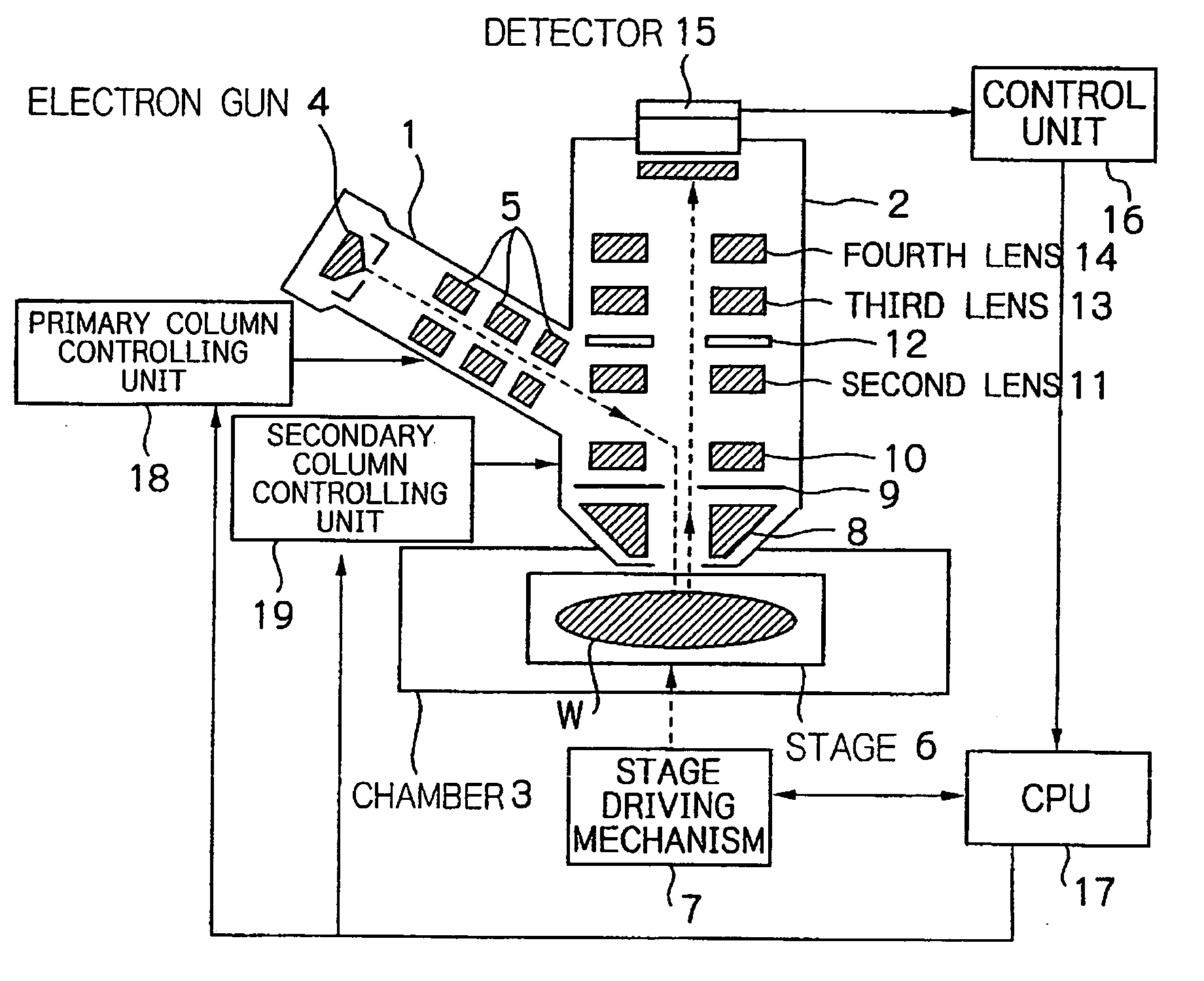
[0058]FIG. 1 is a general view of the image projection type electron beam inspection system according to this embodiment. It should be noted, however, that part of the arrangement is omitted in the illustration.

[0059] In FIG. 1, the electron beam inspection system has a primary column 1, a secondary column 2, and a chamber 3. An electron gun 4 is provided in the primary column 1. A primary optical system 5 is disposed on the optical axis of an electron beam (primary beam) emitted from the electron gun 4. A stage 6 is installed in the chamber 3. A sample W is placed on the stage 6.

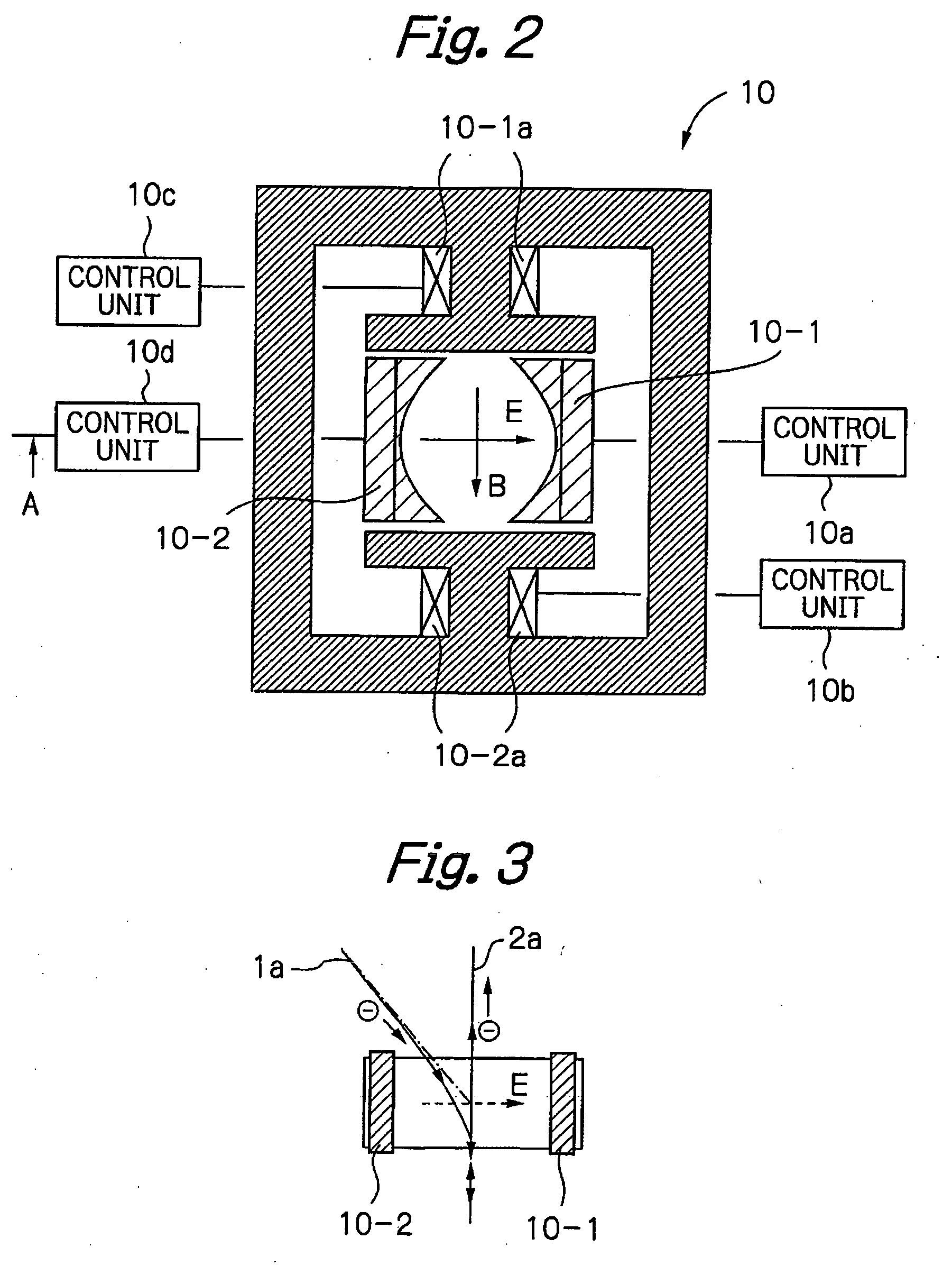
[0060] Meanwhile, the secondary column 2 contains a cathode lens 8, a numerical aperture 9, a Wien filter 10, a second lens 11, a...


PUM


Abstract

An electron beam inspection system of the image projection type includes a primary electron optical system for shaping an electron beam emitted from an electron gun into a rectangular configuration and applying the shaped electron beam to a sample surface to be inspected. A secondary electron optical system converges secondary electrons emitted from the sample. A detector converts the converged secondary electrons into an optical image through a fluorescent screen and focuses the image to a line sensor. A controller controls the charge transfer time of the line sensor at which the picked-up line image is transferred between each pair of adjacent pixel rows provided in the line sensor in association with the moving speed of a stage for moving the sample.

Description

BACKGROUND OF THE INVENTION [0001] The present invention relates to an inspection system for inspecting an object, e.g. a wafer, by using an electron beam to detect a defect or the like in a pattern formed on the surface of the sample under inspection. More particularly, the present invention relates to an inspection system and inspection method wherein an electron beam is irradiated to the surface of an object under inspection, and image data is obtained from the number of secondary electrons emitted from the sample surface, which varies according to the properties of the sample surface, and a pattern or the like formed on the sample surface is inspected with high throughput on the basis of the image data, as in the case of detecting defects on a wafer in the semiconductor fabrication process. The present invention also relates to a method of fabricating devices at high yield by using the inspection system. [0002] Semiconductor fabrication processes are going to enter a new era whe...

Claims


Application Information

Patent Timeline
Patent Type & Authority Applications(United States)
IPC IPC(8): G21K7/00H01J37/22H01J37/244H01J37/28
CPCH01J37/224H01J37/244H01J37/28H01J2237/006H01J2237/20221H01J2237/2445H01J2237/2817
Inventor WATANABE, KENJISOBUKAWA, HIROSINOJI, NOBUHARUSATAKE, TOHRUYOSHIKAWA, SHOJIKARIMATA, TSUTOMUNAKASUJI, MAMORUHATAKEYAMA, MASAHIROMURAKAMI, TAKESHIYAMAZAKI, YUICHIRONAGAHAMA, ICHIROTANAGAI, TAKAMITSUSUGIHARA, KAZUYOSHI
Owner TOSHIBA MEMORY CORP
Why Eureka
Try Eureka