Assembly structure and method for embedded passive device

a passive device and assembly structure technology, applied in the direction of printed circuit aspects, sustainable manufacturing/processing, final product manufacturing, etc., can solve the problems of circuit layout limitation, electrical signal propagation decline, etc., and achieve the effect of enhancing convenience and efficiency and substantially reducing environmental pollution

Inactive Publication Date: 2006-06-08
VIA TECH INC
View PDF2 Cites 68 Cited by
  • Summary
  • Abstract
  • Description
  • Claims
  • Application Information

AI Technical Summary

Benefits of technology

[0011] The present invention uses a method and structure to vertically dispose the passive device so that the passive device can be disposed in the core layer which has available space. Then, a filling material covers the passive device to fix the passive device in the through hole of the core layer. Accordingly, for the availability of the circuit substrate area, the embedded passive device does not occupy the layout area of the internal circuit of the substrate. In addition, by using the present substrate manufacturing process, the assembly process for the vertically embedded passive device can be added thereon to enhance convenience and efficiency. Without using the Sn / Pb solder paste, the environmental pollution can be substantially reduced.

Problems solved by technology

Therefore, the signal transmission route is increased such that the electrical signal propagation declines.
It is a limitation and an inconvenience in the circuit layout.

Method used


Image

  • Assembly structure and method for embedded passive device
  • Assembly structure and method for embedded passive device
  • Assembly structure and method for embedded passive device

Examples


Embodiment Construction

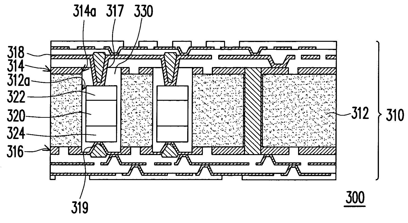
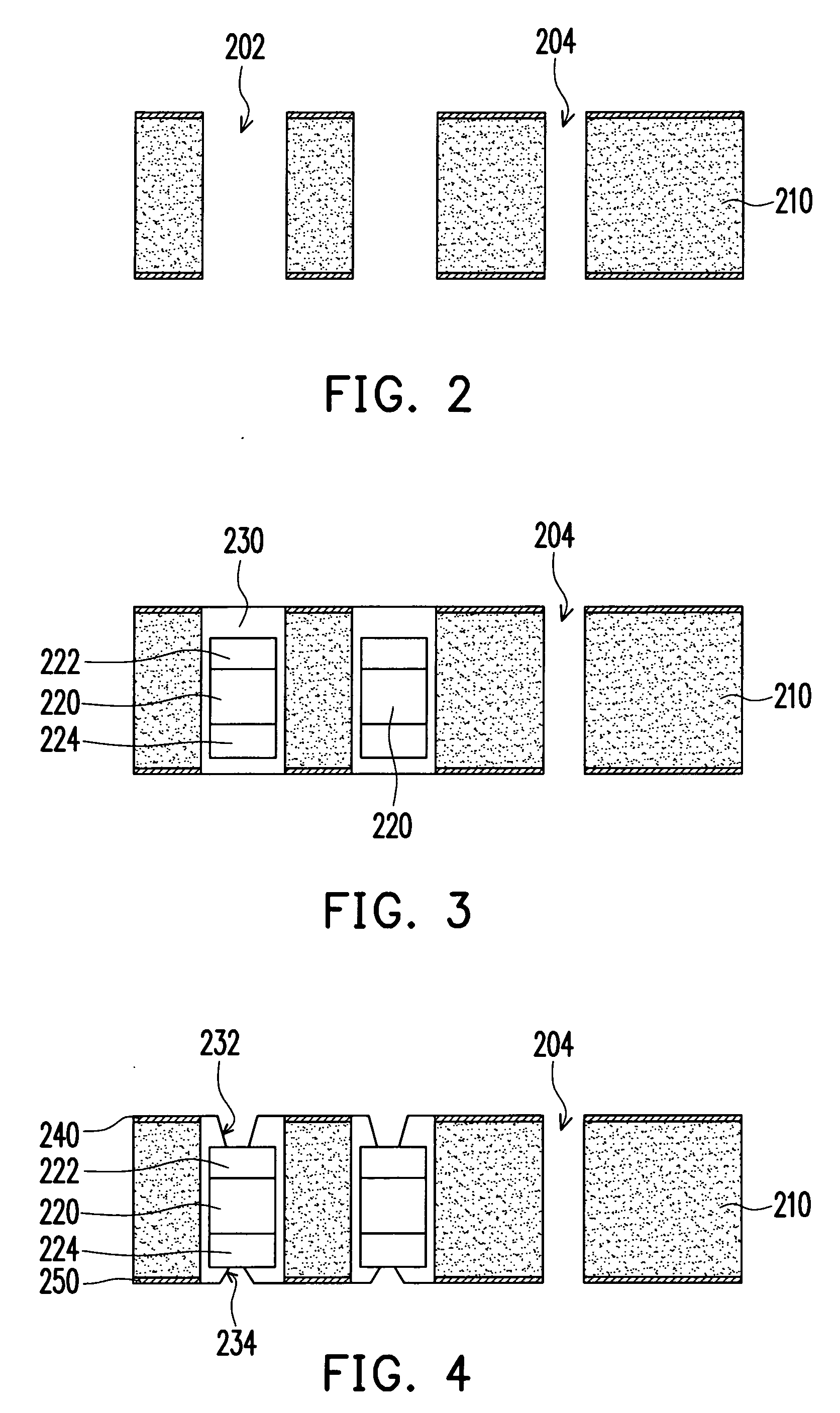
[0018]FIGS. 2-8 are schematic drawings showing progression of an assembly method for an embedded passive device according to an embodiment of the present invention. The assembly process for the embedded passive device is adapted for a circuit substrate. The assembly process comprises the following steps: S110, S120, S130, S140 and S150. First, at least one through hole is pre-formed in a core layer of the circuit substrate in step S110. In step S120, a passive device is disposed in the through hole, and the electrodes of the passive device are correspondingly located on the top and bottom of the through hole. In step S130, a dielectric material is filled in the through hole to cover the passive device. A portion of the dielectric material is removed to expose the electrodes of the passive device in the plural concaves of the dielectric layer. In step S140, a first conductive via and a second conductive via are formed to cover the concaves, respectively. The first conductive layer an...


PUM


Abstract

An assembly structure for an embedded passive device is provided, including at least one passive device embedded in a through hole of a core layer in a circuit substrate. The embedded passive device comprises plural electrodes, which electrically connect through the top side and the bottom side of the core layer. Because the vertically embedded passive device does not occupy the layout area of internal circuit of the circuit substrate, the layout area of the circuit substrate can be increased, the signal transmission route can be reduced, and the performance of signal transmission can be enhanced.

Description

CROSS-REFERENCE TO RELATED APPLICATION [0001] This application claims the priority benefit of Taiwan application serial no. 93137323, filed on Dec. 3, 2004. All disclosure of the Taiwan application is incorporated herein by reference. BACKGROUND OF THE INVENTION [0002] 1. Field of the Invention [0003] The present invention relates to an assembly structure of an embedded passive device, and more particular to an assembly structure and a process to vertically dispose an embedded passive device in a circuit substrate. [0004] 2. Description of the Related Art [0005] Generally, a circuit substrate comprises multiple patterned circuit layers and dielectric layers which are alternatively stacked over each other. Wherein, the patterned circuit layers are made of, for example, copper foils which are defined by a photolithographic process. The dielectric layer is disposed between the patterned circuit layers to isolate the patterned circuit layers. In addition, the stacked patterned circuit l...

Claims


Application Information

Patent Timeline
Patent Type & Authority Applications(United States)
IPC IPC(8): H01L23/02
CPCH01L23/49822H01L23/49827H01L2224/73204H01L2224/32225H01L2224/16225H01L2924/01078H05K1/023H05K1/185H05K3/4602H05K2201/10636H01L2924/01087H01L2924/00012Y02P70/50
Inventor HO, KWUN-YAOKUNG, MORISS
Owner VIA TECH INC
Why Eureka
Try Eureka