PLL circuit

a technology of pll circuit and pll, which is applied in the direction of pulse automatic control, frequency analysis, electric pulse generator, etc., can solve the problems of stringent adjustment width limitations and reduced adjustment range of offset, so as to reduce the adjustment range of offset and reduce the phase offset. , the effect of reducing the phase offs

Inactive Publication Date: 2006-06-08
LONGITUDE LICENSING LTD
View PDF10 Cites 23 Cited by
  • Summary
  • Abstract
  • Description
  • Claims
  • Application Information

AI Technical Summary

Benefits of technology

[0024] If a DC (direct current) based correction means, employing a replica charge pump, is to be provided in the PLL circuit in order to reduce the current offset of the charge pump circuit, there is presented such a problem that, under the effect of the rise time of an output signal of a phase frequency detection circuit or due to use of a lower voltage value of the power supply, adjustment width limitations tend to be stringent, while the adjustable range of the offset tend...

Problems solved by technology

If a DC (direct current) based correction means, employing a replica charge pump, is to be provided in the PLL circuit in order to reduce the current offset of the charge pump circuit, there is presented such a problem that, under the effect ...

Method used


Image

  • PLL circuit
  • PLL circuit
  • PLL circuit

Examples


Embodiment Construction

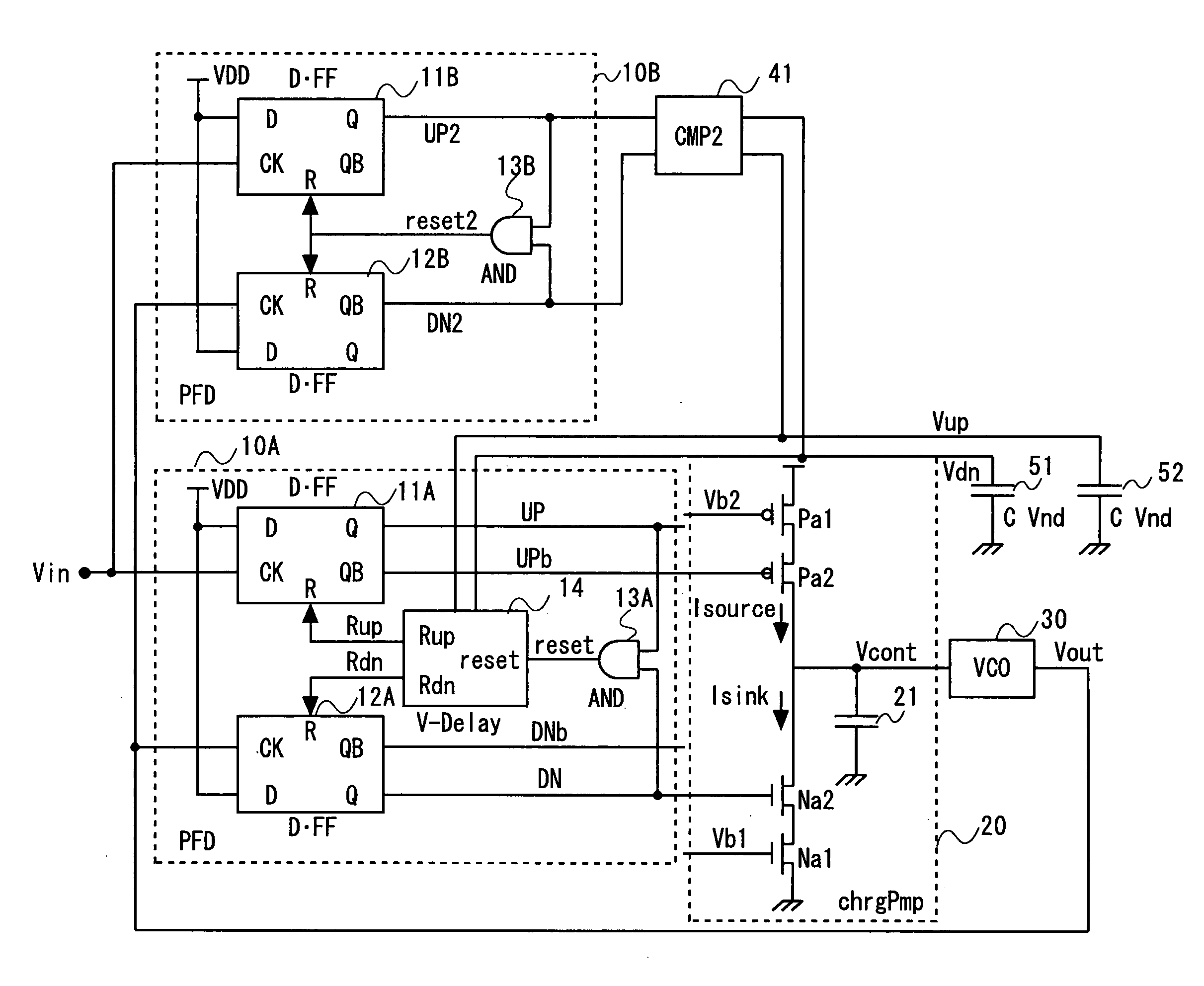
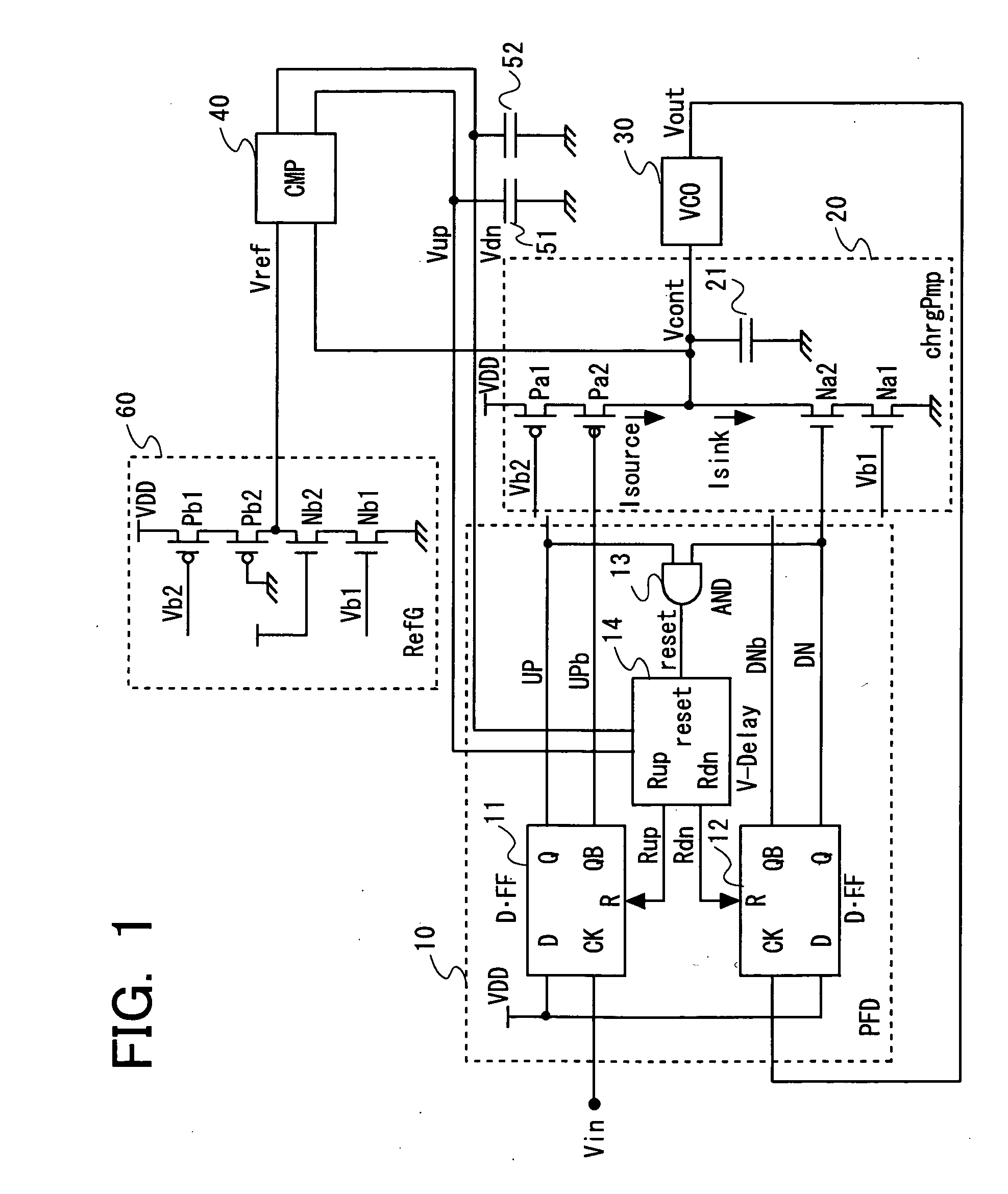
[0058] Referring to the drawings, certain preferred embodiments of the present invention will be described in detail. Referring to FIG. 1, the PLL circuit according to an embodiment of the present invention includes a phase frequency detector (10) for comparing phase and frequency between an input clock signal and a feedback output signal, a charge pump circuit (20) for generating a control signal corresponding to the result of comparison of the phase frequency detector, and a voltage-controlled oscillator (30) for generating an output signal of a frequency complying with the control voltage. The output signal of the voltage-controlled oscillator (30) is supplied as the feedback output signal to an input of the phase frequency detector (10). The present invention may as a matter of course adopt such a configuration in which the output signal of the voltage-controlled oscillator (30) is supplied to a frequency-divider not shown which is provided in the feedback path and the frequency...


PUM


Abstract

Disclosed is a PLL circuit including a phase frequency detector (PFD) for comparing phase and frequency between an input signal and an output signal, a charge pump circuit for charging a capacitor when an up-signal from the PFD is activated, discharging the capacitor when a down-signal is activated, and for outputting the terminal voltage of the capacitor as a control voltage, and a VCO for outputting an output signal of a frequency in accordance with the control voltage. An output of the VCO is fed back as an output signal to the PFD as input. The PFD includes a delay adjustment circuit for exercising control for resetting the up-signal and the down-signal with a preset delay as from a time point both up-signal and the down-signal have been activated. There is also provided a comparator amplifier circuit for comparing a reference voltage, corresponding to a control voltage when both up-signal and down-signal are activated, to supply first and second control signals to the delay adjustment circuit. The pulse widths of up and down-signals are adjusted depending on current offset characteristics of the charge pump circuit.

Description

FIELD OF THE INVENTION [0001] This invention relates to a PLL circuit and, more particularly, to a circuit configuration that may be suitably applied to a charge-pump type PLL circuit. BACKGROUND OF THE INVENTION [0002] Recently, with the increase of operating speed (operating clock frequency) of CMOS LSI products, larger numbers of LSI products, each having a PLL (phase-locked loop) circuit, are manufactured and sold. The degree of accuracy demanded of the PLL circuit nowadays has become increasingly higher. [0003] In the conventional charge-pump type PLL circuit, phase offset persists, so that variations in for example, temperature, power supply voltage, or fabrication process, significantly affect the circuit characteristic of the PLL circuit. Hence, the improvement of this situation in the charge-pump type PLL circuit is required. [0004]FIG. 10 is a diagram illustrating an example of the configuration of a conventional charge-pump type PLL circuit (see Non-Patent Document 1). Re...

Claims


Application Information

Patent Timeline
IPC IPC(8): H03L7/06
CPCH03L7/081H03L7/087H03L7/0891H03L7/0995Y10S331/02
Inventor KOBAYASHI, SHOTARO
Owner LONGITUDE LICENSING LTD
Why Eureka
Try Eureka