Imaging apparatus and imaging method

Inactive Publication Date: 2006-06-08
GK BRIDGE 1
View PDF22 Cites 37 Cited by
  • Summary
  • Abstract
  • Description
  • Claims
  • Application Information

AI Technical Summary

Benefits of technology

[0021] Areas containing pixels where the image signal changes greatly between temporally consecutive frames are areas containing much movement, or more particularly containing a moving subject. Increasing the resolution in these areas can improve image defi

Problems solved by technology

Reading this many pixels in such a short time is very difficult at the operating rate of current image se

Method used


Image

  • Imaging apparatus and imaging method
  • Imaging apparatus and imaging method
  • Imaging apparatus and imaging method

Examples


embodiment 1

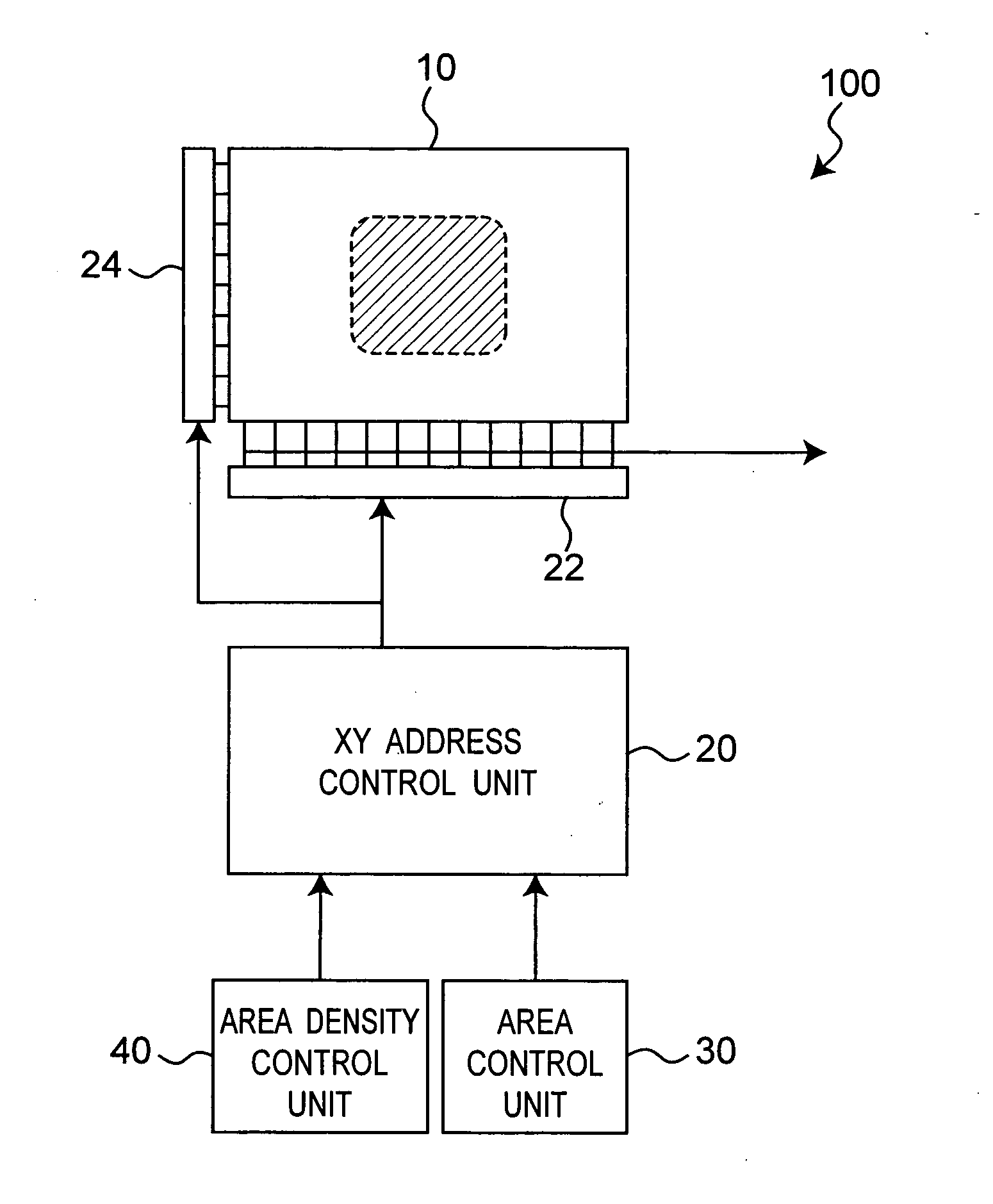
[0051] An imaging apparatus 100 according to a first embodiment of the present invention is described below with reference to FIG. 1 to FIG. 7. FIG. 1 is a block diagram of an imaging apparatus 100 according to this first embodiment of the invention.

[0052] As shown in FIG. 1, this imaging apparatus 100 has an image sensor 10, XY address control unit 20, horizontal selection circuit 22, vertical selection circuit 24, area control unit 30, and area density control unit 40.

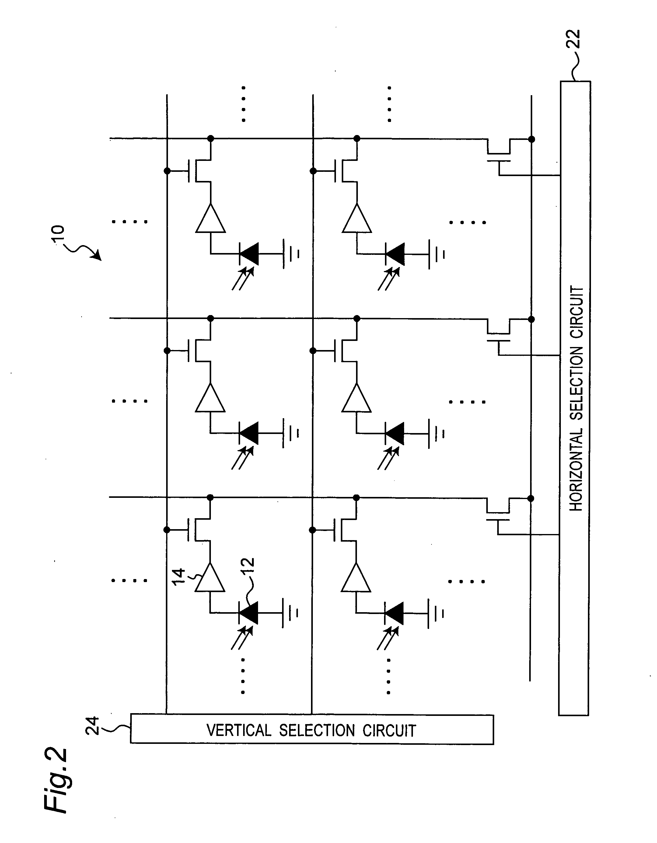
[0053]FIG. 2 is a schematic circuit diagram of the image sensor 10. This image sensor 10 is a CMOS image sensor. This CMOS sensor 10 is a two-dimensional array of pixels, each pixel having an element 12 operable to produce an electric charge by photoelectrically converting light from an imaged subject, and a part 14 operable to accumulate the produced charge and output a signal representing the accumulated charge. The elements 12 that photoelectrically convert light to produce a charge are called photodiodes. Each ...

embodiment 2

[0151] An imaging apparatus according to a second embodiment of the present invention is described next with reference to FIG. 20 to FIG. 23. This imaging apparatus 200 differs from the imaging apparatus of the first embodiment in pre-segmenting the total area of the image sensor 10a into a plurality of areas (area 0 to area 11 in this example), and the area density control unit 40 setting the density of pixels read from each area. The imaging apparatus 200 of this embodiment thus differs from the first imaging apparatus 100 described above in not having an area control unit because the total image area is already segmented into a plurality of areas.

[0152]FIG. 20 is a block diagram of this imaging apparatus 200. As shown in FIG. 21, the image sensor 10a is segmented into a 4×3 matrix of twelve areas, area 0 to area 11. Proceeding left to right, top to bottom from the top left area, these areas are identified sequentially from area 0, area 1, area 2 to area 11. Each area contains 17...


PUM


Abstract

The resolution, frame rate, or both can be improved when imaging moving subjects in an imaging apparatus using a CMOS image sensor. The imaging apparatus has an image sensor having a two-dimensional array of pixels. Each of the pixels includes an element operable to produce an electric charge by photoelectrically converting light from an imaged subject and a part operable to accumulate the produced charge and output an accumulated charge or a signal representing the accumulated charge. The imaging apparatus also has an area control unit operable to define a specified area of the image sensor containing a plurality of pixels and an area density control unit operable to specify a density of pixels read from the specified area defined by the area control unit.

Description

BACKGROUND OF THE INVENTION [0001] 1. Field of Technology [0002] The present invention relates to an imaging apparatus using a MOS solid state imaging element, and to an imaging method. [0003] 2. Description of Related Art [0004] Solid state imaging elements (image sensors) are used to convert light from a subject to an electric signal in digital cameras, video cameras, and other imaging devices used in applications for capturing and storing images. Solid state imaging elements mainly include CCD image sensors and MOS image sensors. CCD image sensors are more common today, however, because of such features as a wide dynamic range and isochronous imaging performance. Disadvantages to CCD image sensors include high power consumption and the need for different power supply voltages, and further significant improvement in these characteristics is not expected. [0005] MOS image sensors have a narrower dynamic range and are more susceptible to noise than CCD image sensors, but recent rese...

Claims


Application Information

Patent Timeline
IPC IPC(8): H04N1/04
CPCH04N3/1512H04N3/1562H04N5/23212H04N25/443H04N25/445H04N25/46H04N25/76
Inventor CHIBA, TAKUMAOKAMOTO, KAZUONAGAISHI, YUJIJURI, TATSURO
Owner GK BRIDGE 1
Why Eureka
Try Eureka