Transistor using impact ionization and method of manufacturing the same

a technology of impact ionization and transistor, which is applied in the field of transistors, can solve the problems of difficult to lower the subthreshold slope below 60 mv/decade at room temperature, limited miniaturization of transistors, and difficult to use self-alignmen

Inactive Publication Date: 2006-06-15
ELECTRONICS & TELECOMM RES INST
View PDF3 Cites 38 Cited by
  • Summary
  • Abstract
  • Description
  • Claims
  • Application Information

AI Technical Summary

Benefits of technology

[0019] The present invention provides an impact-ionization transistor, which can overcome the limit of a metal-oxide semiconductor field effect transistor (MOSFET) in miniaturization and allow self-alignment, and a method of manufacturing the same.

Problems solved by technology

However, in the operating principle of a metal-oxide semiconductor field effect transistor (MOSFET), it is difficult to lower a subthreshold slope below 60 mV / decade at room temperature.
Accordingly, miniaturization of a transistor is limited.
However, since it is needed to respectively use opposite types of impurities for the source 34 and the drain 35 and to form the I-region 37 having an offset in the conventional I-MOSFET, it is difficult to use self-alignment.
However, leakage current is large due to the bulk substrate 51.
In addition, the conventional I-MOSFET using a sidewall is disadvantageous in developing commercial processes and designing a circuit since it has a different structure than normal MOSFETs.

Method used


Image

  • Transistor using impact ionization and method of manufacturing the same
  • Transistor using impact ionization and method of manufacturing the same
  • Transistor using impact ionization and method of manufacturing the same

Examples


Embodiment Construction

[0031] The present invention will now be described more fully with reference to the accompanying drawings, in which exemplary embodiments of the invention are shown. The invention may, however, be embodied in many different forms and should not be construed as being limited to the embodiments set forth herein; rather, these embodiments are provided so that this disclosure will be thorough and complete, and will fully convey the concept of the invention to those skilled in the art.

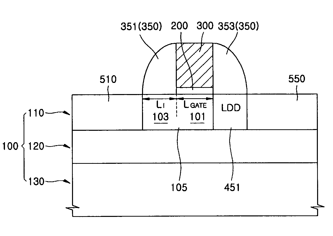
[0032] In embodiments of the present invention, an impact-ionization transistor including a source with schottky junction and a method of manufacturing the same are provided. An impact-ionization transistor according to an embodiment of the present invention may include a first drain region, i.e., a lightly doped drain (LDD) region facing the source, a second drain region preferably including silicide at the back of the first drain region, an ionization region (I-region) below an offset sidewall spacer adj...


PUM


Abstract

A transistor using impact ionization and a method of manufacturing the same are provided. A gate dielectric layer, a gate, and first and second spacers are formed on a semiconductor substrate. A first impurity layer is formed spaced from the first spacer and a second impurity layer is formed expanding and overlapping with the second spacer therebelow, by performing slant ion-implantation on the semiconductor substrate using the gate and the first and second spacers as a mask. A source and a drain are formed on the semiconductor substrate to be self-aligned with the first and second spacers, respectively, thereby defining an ionization region between the source and the drain in the semiconductor substrate. The source includes a first silicide layer to form a schottky junction with the ionization region. The drain includes a portion of the second impurity layer overlapping with the second spacer and a second silicide layer which is aligned with the second spacer to form an ohmic contact with the second impurity layer.

Description

CROSS-REFERENCE TO RELATED PATENT APPLICATIONS [0001] This application claims the benefit of Korean Patent Application Nos. 10-2004-0105430, filed on Dec. 14, 2004, and No. 10-2005-034030, filed on Apr. 25, 2005, in the Korean Intellectual Property Office, the disclosure of which is incorporated herein in its entirety by reference. BACKGROUND OF THE INVENTION [0002] 1. Field of the Invention [0003] The present invention relates to a semiconductor device, and more particularly, to a transistor controlling a breakdown voltage of a junction using impact ionization and a method of manufacturing the same. [0004] 2. Description of the Related Art [0005] With the development of semiconductor technology, needs on high-performance and high-density device have increased. A typical transistor is designed to operate according to the Fermi-Dirac distribution and drift-diffusion of carriers. However, in the operating principle of a metal-oxide semiconductor field effect transistor (MOSFET), it is...

Claims


Application Information

Patent Timeline
Patent Type & Authority Applications(United States)
IPC IPC(8): H01L27/095
CPCH01L21/26586H01L21/28052H01L21/28202H01L29/495H01L29/518H01L29/665H01L29/66643H01L29/66659H01L29/7835H01L29/7839
Inventor YANG, JONG HEONBAEK, IN BOKIM, KI JUAHN, CHANG GEUNCHO, WON JULEE, SEONG JAE
Owner ELECTRONICS & TELECOMM RES INST
Why Eureka
Try Eureka