Chalcogenide random access memory and method of fabricating the same

a random access memory and chalcogenide technology, applied in the direction of basic electric elements, electrical equipment, semiconductor devices, etc., can solve the problem of quite limited current that can be provided by transistors, and achieve the effect of reducing differences

Active Publication Date: 2006-06-22
MACRONIX INT CO LTD
View PDF3 Cites 21 Cited by
  • Summary
  • Abstract
  • Description
  • Claims
  • Application Information

AI Technical Summary

Benefits of technology

[0008] Accordingly, at least one objective of the present invention is to provide a chalcogenide random access memory (CRAM) capable of reducing the difference between an operating current of the CRAM and a current provided by a control transistor.
[0009] At least another objective of the present invention is to provide a chalcogenide random access memory (CRAM) that can reduce the driving current of the CRAM.
[0010] At least another objective of the present invention is to provide a chalcogenide random access memory (CRAM) that can reduce the operating current of the CRAM and ignore the difference in the thermal expansion coefficient between the chalcogenide material and other materials used in semiconductor production.

Problems solved by technology

However, the current that can be provided by a transistor is quite limited.
Hence, one major issue is to achieve a balance between the operating current of the chalcogenide RAM and the current range provided by the transistor.

Method used


Image

  • Chalcogenide random access memory and method of fabricating the same
  • Chalcogenide random access memory and method of fabricating the same
  • Chalcogenide random access memory and method of fabricating the same

Examples


first embodiment

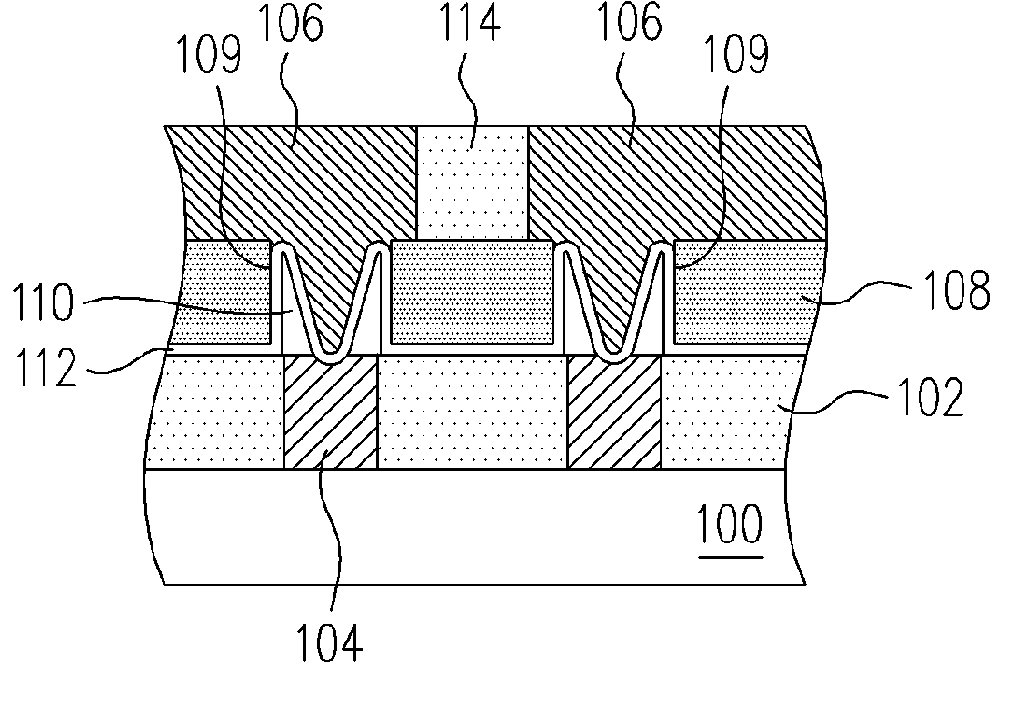
[0036]FIG. 1 is a schematic cross-sectional view of a chalcogenide random access memory according to the present invention. As shown in FIG. 1, the chalcogenide random access memory (CRAM) of the present embodiment mainly comprises a substrate 100, a first dielectric layer 102, a bottom electrode 104, a top electrode 106, a second dielectric layer 108, a modified chalcogenide spacer 110 and a un-modified chalcogenide thin film 112. The first dielectric layer 102 is disposed on the substrate 100 and the bottom electrode 104 is located inside the first dielectric layer 102. The second dielectric layer 108 is disposed on the first dielectric layer 102, wherein the second dielectric layer 108 has at least one opening 109 exposing the bottom electrode 104. The modified chalcogenide spacer 110 is disposed on the sidewall of the opening 109 exposing portion of the bottom electrode 104. The top electrode 106 is disposed on the bottom electrode 104. The un-modified chalcogenide thin film 112...

second embodiment

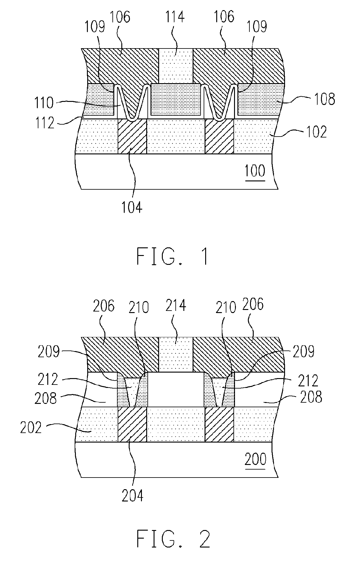
[0039]FIG. 2 is a schematic cross-sectional view of a chalcogenide random access memory according to the present invention. As shown in FIG. 2, the chalcogenide random access memory (CRAM) in the present embodiment mainly comprises a substrate 200, a dielectric layer 202, a bottom electrode 204, a top electrode 206, a modified chalcogenide layer 208, a spacer 210 and a un-modified chalcogenide material 212. The dielectric layer 202 is disposed on the substrate 200 and the bottom electrode 204 is located inside the dielectric layer 202. The modified chalcogenide layer 208 is disposed on the dielectric layer 202, wherein the modified chalcogenide layer 208 has at least one opening 209 exposing the bottom electrode 204. The spacer 210 is disposed on the sidewall of the opening 209 so as to expose portion of the bottom electrode 204, wherein the spacer 210 can be fabricated using a dielectric or a insulator. The top electrode 206 is disposed on the bottom electrode 204. The un-modified ...

fourth embodiment

[0044]FIG. 4A through 4H are schematic cross-sectional views showing the steps for fabricating a chalcogenide random access memory according to the present invention. As shown in FIG. 4A, a substrate 400 having a first dielectric layer 402 thereon is provided. Furthermore, the first dielectric layer 402 has a bottom electrode 404 therein.

[0045] Thereafter, as shown in FIG. 4B, a chalcogenide film 406 is formed over the substrate 400 and then a patterned mask 408 is formed over the chalcogenide film 406. The patterned mask 408 is a photoresist layer or a hard mask, for example.

[0046] As shown in FIG. 4C, the chalcogenide film 406 (as shown in FIG. 4B) is patterned using the pattern mask 408 to form a chalcogenide block 406a in contact with the bottom electrode 404.

[0047] As shown in FIG. 4D, using the patterned mask 408 again, a tilt ion implantation process 410 is performed on the chalcogenide block 406a so that a peripheral portion of the contact area between the chalcogenide blo...


PUM


Abstract

A chalcogenide random access memory (CRAM) is provided. The CRAM includes a substrate, a first dielectric layer, a bottom electrode, a top electrode, a second dielectric layer, a modified chalcogenide spacer and an un-modified chalcogenide thin film. The first dielectric layer is disposed on the substrate and the bottom electrode is located inside the first dielectric layer. The second dielectric layer is disposed on the first dielectric layer and it has at least one opening exposing the bottom electrode. The modified chalcogenide spacer is disposed on the sidewall of the opening exposing portion of the bottom electrode. The top electrode is disposed on the bottom electrode. The un-modified chalcogenide thin film is disposed between the modified chalcogenide spacer and the top electrode and also disposed between the bottom electrode and the top electrode. The modified chalcogenide spacer has a better etching resistivity than the un-modified chalcogenide thin film.

Description

CROSS-REFERENCE TO RELATED APPLICATION [0001] This application is a continuation-in-part of a prior application Ser. No. 10 / 905,115, filed Dec. 16, 2004.BACKGROUND OF THE INVENTION [0002] 1. Field of the Invention [0003] The present invention relates to a phase transformation memory and fabricating method thereof. More particularly, the present invention relates to a chalcogenide random access memory (CRAM) and method of fabricating the same. [0004] 2. Description of the Related Art [0005] To satisfy the need for varieties, compactness, high density, low production cost and customization in memory products, an increasing large list of memory fabrication techniques are being investigated. One type of technique that receives particular attention is a phase-transformation memory. Phase-transformation is a process of changing a material from a non-crystalline state into a crystalline state or changing the crystalline state to a non-crystalline state. Because a non-crystalline material h...

Claims


Application Information

Patent Timeline
Patent Type & Authority Applications(United States)
IPC IPC(8): H01L29/768H01L29/04H01L45/00
CPCH01L45/06H01L45/1233H01L45/165H01L45/1273H01L45/1246H01L29/04H01L21/425H10N70/828H10N70/8418H10N70/231H10N70/043H10N70/826H01L29/768H10N70/00
Inventor HSUEH, MING-HSIANG
Owner MACRONIX INT CO LTD
Why Eureka
Try Eureka