Multi-level semiconductor module

Inactive Publication Date: 2006-06-22
PANASONIC CORP
View PDF6 Cites 10 Cited by
  • Summary
  • Abstract
  • Description
  • Claims
  • Application Information

AI Technical Summary

Benefits of technology

[0010] In recent years, techniques for reducing the thickness of semiconductor chips by polishing and techniques for mounting the thin semiconductor chips on boards with high yields have been developed, so that the number of levels of such stacked semiconductor chips has been further increasing. In addition, in a semiconductor memory, for example, as the memory capacity increases, the chip area increases. If a module is formed by stacking large semiconductor chips in multiple levels, the problem of a warp of the module arises. The degree of warp of the module increases as the thickness of a printed board decreases. Accordingly, to stack printed boards on which semiconductor chips are mounted and interlayer members in multiple levels, it is important to suppress the occurrence of a warp.

Problems solved by technology

If a module is formed by stacking large semiconductor chips in multiple levels, the problem of a warp of the module arises.
Accordingly, if a warp occurs at room temperature or is caused by heating during bonding, a semiconductor module cannot be mounted on the mother board or the warp causes a partial failure in packaging.
That is, a semiconductor module can be defective in packaging though it is non-defective in its electric characteristics.

Method used


Image

  • Multi-level semiconductor module
  • Multi-level semiconductor module
  • Multi-level semiconductor module

Examples


embodiment 1

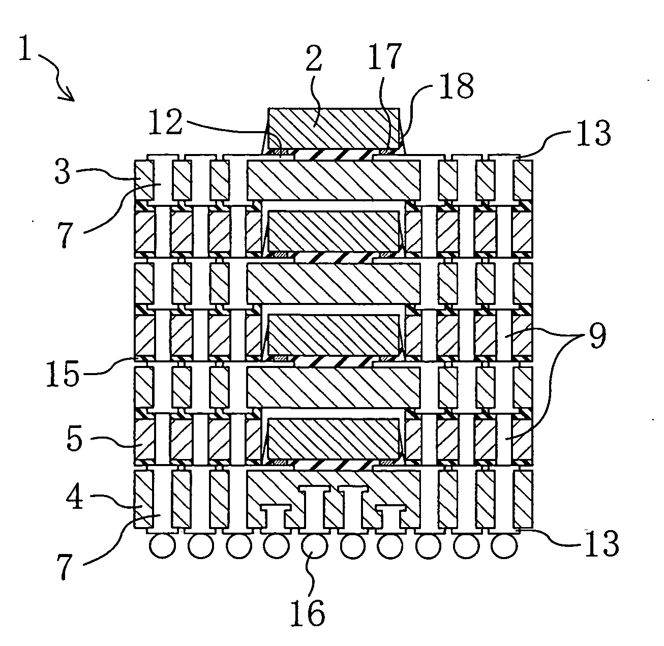
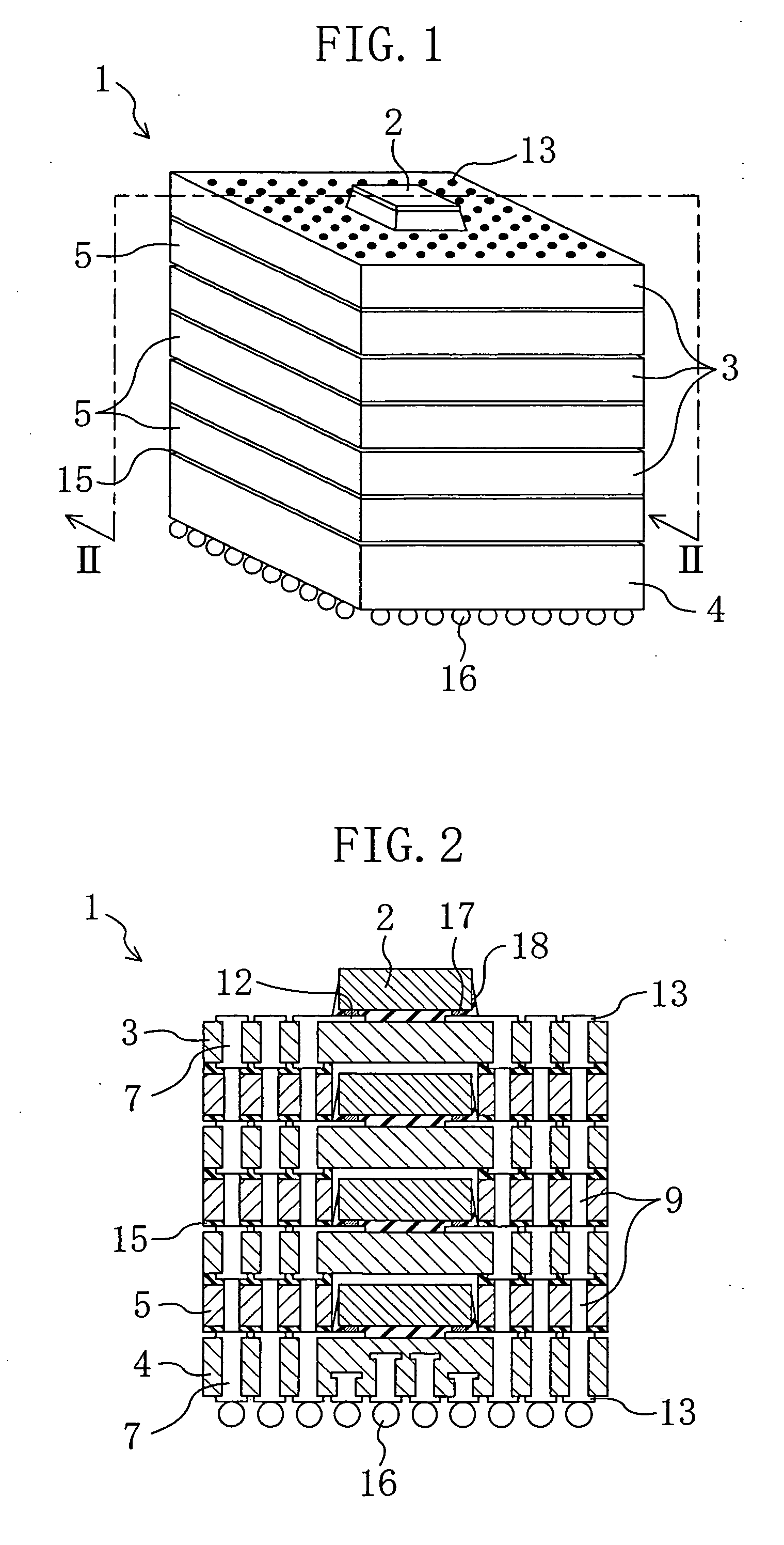
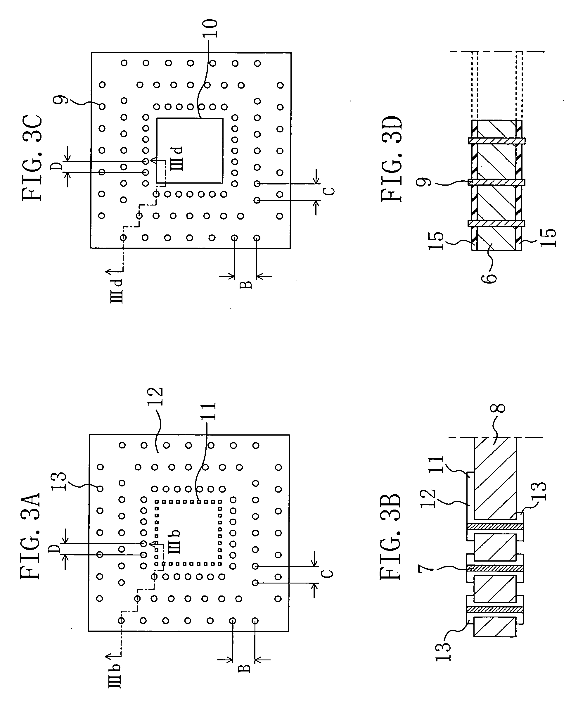
[0039] A multi-level semiconductor module according to a first embodiment of the present invention will be described with reference to FIGS. 1, 2 and 3A through 3D.

[0040]FIG. 1 is a perspective view schematically illustrating an overall structure of a semiconductor module 1 according to each embodiment of the present invention. FIG. 2 is a cross-sectional view of the semiconductor module 1 taken along the line II-II in FIG. 1. FIGS. 3A and 3C are plan views illustrating a first resin board 3 and a sheet member 5, respectively, for use in the semiconductor module 1 of this embodiment. FIG. 3B is a cross-sectional view of the first resin board 3 taken along the line IIIb-IIIb. FIG. 3D is a cross-sectional view of the sheet member 5 taken along the line IIId-IIId. In these drawings, the thicknesses, lengths and shapes of parts of the semiconductor module are selected so as to be easily shown, and therefore are different from those of actual parts. The shapes and numbers of buried cond...

embodiment 2

[0059] A multi-level semiconductor module according to a second embodiment of the present invention will be described with reference to FIGS. 1, 2, and 4A through 4D. FIGS. 4A and 4C are plan views illustrating a first resin board 3 and a sheet member 5, respectively, for use in a semiconductor module 1 according to this embodiment. FIG. 4B is a cross-sectional view of the first resin board 3 taken along the line IVb-IVb. FIG. 4D is a cross-sectional view of the sheet member 5 taken along the line IVd-IVd.

[0060] As illustrated in FIGS. 1 and 2, the semiconductor module of this embodiment is the same as that of the first embodiment except for the arrangement of first buried conductors 7 and second buried conductors 9, and thus description of components already described in the first embodiment will be omitted.

[0061] As illustrated in FIG. 4A, the first buried conductors 7 are basically symmetrical laterally and vertically in plan view in first resin boards 3 and a second resin boar...

embodiment 3

[0065] A multi-level semiconductor module according to a third embodiment of the present invention will be described with reference to FIGS. 1, 2, and 5A through 5D. FIGS. 5A and 5C are plan views illustrating a first resin board 3 and a sheet member 5, respectively, for use in a semiconductor module 1 according to this embodiment. FIG. 5B is a cross-sectional view of the first resin board 3 taken along the line Vb-Vb. FIG. 5D is a cross-sectional view of the sheet member 5 taken along the line Vd-Vd.

[0066] As illustrated in FIGS. 1 and 2, the semiconductor module of this embodiment is the same as that of the first embodiment except for the arrangements and diameters of first buried conductors 7 and second buried conductors 9, and thus description of the same components will be omitted.

[0067] As illustrated in FIG. 5A, the first buried conductors 7 are basically symmetrical laterally and vertically in plan view in first resin boards 3 and a second resin board 4 of this embodiment....


PUM


Abstract

A semiconductor module is formed by alternately stacking resin boards on which semiconductor chips are mounted and sheet members having openings larger than the semiconductor chips and bonded to the resin boards. One of the resin boards located at the bottom has a thickness larger than that of each of the other resin boards. First buried conductors formed in each of first resin boards are arranged to form a plurality of lines surrounding a region on which a semiconductor chip is to be mounted. The spacing between the first buried conductors increases in succession toward the outermost line. Second buried conductors formed in each of sheet members are arranged to form a plurality of lines surrounding an opening. The spacing between the second buried conductors increases in succession toward the outermost line.

Description

CROSS-REFERENCE TO RELATED APPLICATION [0001] This application claims priority under 35 U.S.C. §119(a) on Patent Application No. 2004-364570 filed in Japan on Feb. 16, 2004, the entire contents of which are hereby incorporated by reference. BACKGROUND OF THE INVENTION [0002] (1) Field of the Invention [0003] The present invention relates to three-dimensional multi-level semiconductor modules formed by alternately stacking sheet members and resin boards on which semiconductor chips are mounted. [0004] (2) Description of the Related Art [0005] With demands for size reduction and performance improvement of various electronic devices such as cellular phones and digital cameras, multi-level semiconductor modules formed by stacking and uniting a plurality of electronic components, especially semiconductor chips, have been proposed. [0006] Methods for easily manufacturing such multi-level semiconductor modules at low cost have been proposed to date. [0007] A conventional semiconductor modu...

Claims


Application Information

Patent Timeline
IPC IPC(8): H01L23/02
CPCH01L25/0657H01L2224/16225H01L2225/06517H01L2225/0652H01L2225/06541H01L2225/06551H01L2225/06572H01L2225/06586H01L2225/06596H01L2924/01078H01L2924/15311H01L2924/3011H01L2224/73204H01L2224/32225H01L2924/00H01L2924/00012H01L2924/1627H01L23/12H01L25/10
Inventor SATOU, MOTOAKIKAWABATA, TAKESHIFUKUDA, TOSHIYUKI
Owner PANASONIC CORP
Why Eureka
Try Eureka