Electron-emitting apparatus

a technology of electron-emitting apparatus and discharge tube, which is applied in the direction of discharge tube main electrode, discharge tube luminescnet screen, nanoinformatics, etc., can solve the problem of large power consumption of the electron-emitting apparatus, and achieve the effect of inhibiting the rectilinear propagation of the electron

Inactive Publication Date: 2006-06-22
NGK INSULATORS LTD
View PDF5 Cites 2 Cited by
  • Summary
  • Abstract
  • Description
  • Claims
  • Application Information

AI Technical Summary

Benefits of technology

[0006] An object of the present invention is to provide an electron-emitting apparatus that can ensure emission of electrons in a target direction with low power consumption.

Problems solved by technology

Thus, the electron-emitting apparatus has a problem of large power consumption.

Method used


Image

  • Electron-emitting apparatus
  • Electron-emitting apparatus
  • Electron-emitting apparatus

Examples


first embodiment

Structure

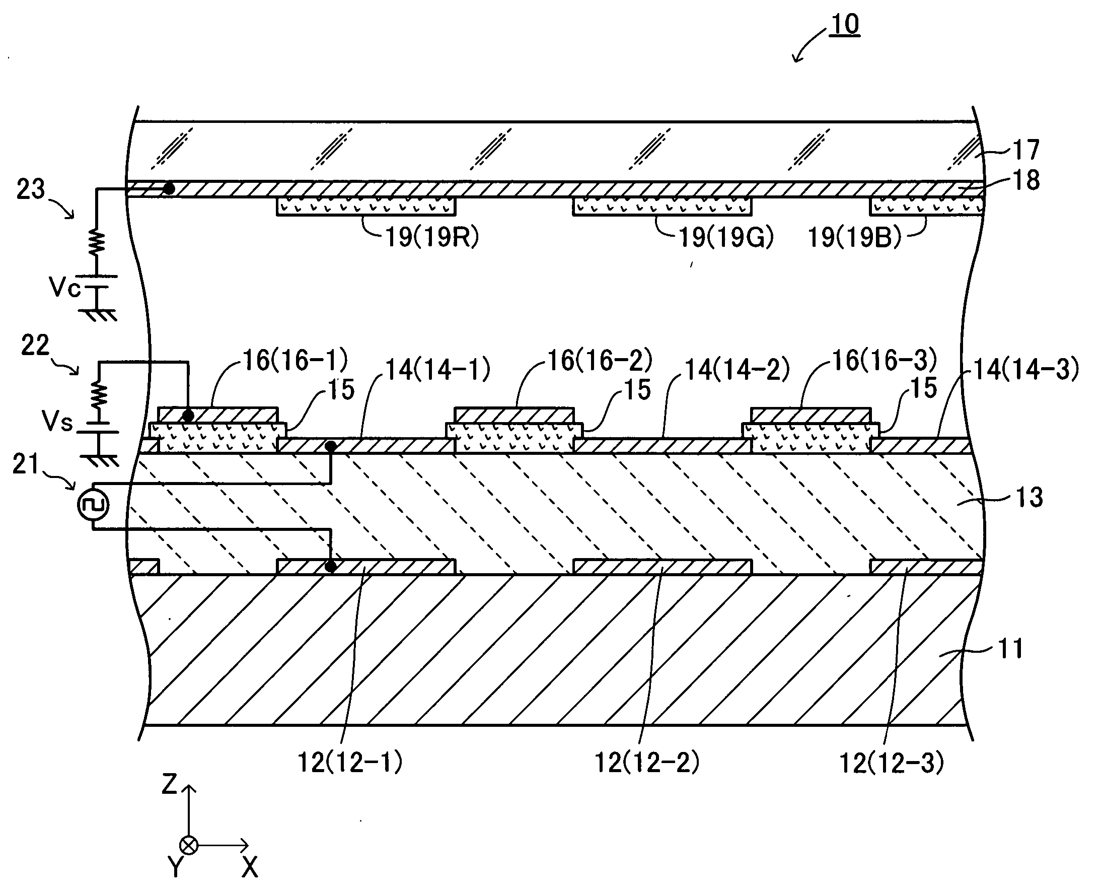
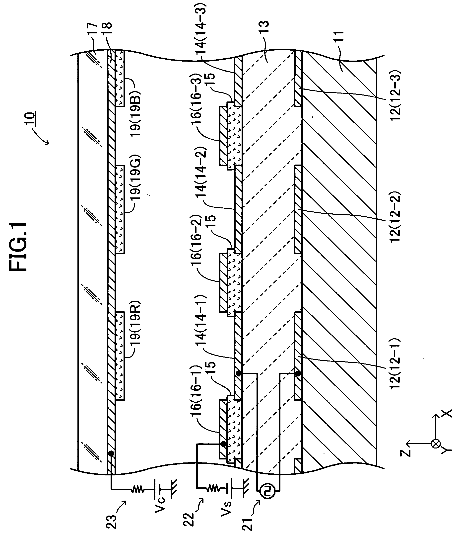
[0069] As shown in FIGS. 1 to 3, an electron emitting apparatus (an electron emitting device) 10 according to a first embodiment of the present invention includes a substrate 11, a plurality of lower electrodes (lower electrode layers) 12, an emitter section 13, a plurality of upper electrodes (upper electrode layers) 14, insulating layers 15, and focusing electrodes (focusing electrode layers, a bundling electrode to bundle emitted electrons) 16. FIG. 1 is a cross-sectional view of the electron emitting apparatus 10 taken along line I-I in FIG. 3, which is a partial plan view of the electron emitting apparatus 10. FIG. 2 is a cross-sectional view of the electron emitting apparatus 10 taken along line II-II in FIG. 3.

[0070] The substrate 11 is a thin plate having an upper surface and a lower surface parallel to the plane (X-Y plane) defined by the X axis and the Y axis perpendicular to each other. The thickness direction of the substrate 11 is the Z-axis direction perpen...

first modification example of first embodiment

[0120] As shown in the plan view of FIG. 16, one pixel PX of a first modification example includes three upper electrodes 14 (a first upper electrode 14-1, a second upper electrode 14-2, and a third upper electrode 14-3) for emitting light of three different colors. The three upper electrodes 14 are aligned in the X-axis direction. As in the first embodiment described above, a red phosphor (not shown) is disposed directly above the first upper electrode 14-1, a green phosphor (not shown) is disposed directly above the second upper electrode 14-2, and a blue phosphor (not shown) is disposed directly above the third upper electrode 14-3. The pixels PX are aligned such that the upper electrodes 14-1 of these pixels are aligned in a column extending in the Y-axis direction and so are the upper electrodes 14-2 and the upper electrodes 14-3. According to this arrangement, the pixels of the display including the electron-emitting apparatus of the first modification example are arranged int...

second modification example of first embodiment

[0122] A display incorporating a second modification example of the electron-emitting apparatus of the present invention will now be described with reference to FIG. 17. In this second modification example, the focusing electrodes 16 are disposed not only between the adjacent upper electrodes 14 in the X-axis direction in the plan view but also between the upper electrodes 14 adjacent in the Y-axis direction. This arrangement is the only difference between the second modification example and the first modification example.

[0123] In the second modification example, as in the first modification example, electrons emitted from the upper electrode 14 of a particular element does not reach the phosphors disposed above the upper electrodes 14 of the other elements adjacent to this particular element in the X-axis direction. Thus, satisfactory color purity can be maintained. Furthermore, in the second modification example, the focusing electrodes 16 are also disposed between the upper ele...


PUM


Abstract

An electron-emitting apparatus includes an emitter section made of a dielectric material, lower electrodes, upper electrodes having micro through holes, insulating layers disposed on the upper surface of the emitter section and between the adjacent upper electrodes, and focusing electrodes to which a predetermine potential is applied and which are disposed on the insulating layers. The electron-emitting apparatus applies a negative potential to the upper electrode to accumulate electrons in the emitter section and then applies a positive potential to the upper electrode. As a result, the polarization of the emitter section is reversed, and the accumulated electrons are emitted through the micro through holes in the upper electrodes by Coulomb repulsion. Owing to electric fields generated by the focusing electrodes, the emitted electrons travel in the upward direction of the upper electrode without spreading into a shape of a cone.

Description

BACKGROUND OF THE INVENTION [0001] 1. Field of the Invention [0002] The present invention relates to an electron-emitting apparatus including an emitter section made of a dielectric material, a lower electrode disposed below the emitter section, and an upper electrode disposed above the emitter section. [0003] 2. Description of the Related Art [0004] In the related art, an electron-emitting apparatus including an emitter section made of a dielectric material, a lower electrode (lower electrode layer) disposed below the emitter section, and an upper electrode (upper electrode layer) disposed above the emitter section and having numerous micro trough holes has been known. According to this type of electron-emitting apparatus, a high-voltage pulse is applied between the upper electrode and the lower electrode to reverse the polarization of the dielectric material and to thereby emit electrons through the micro through holes in the upper electrode (e.g., refer to Japanese Patent No. 316...

Claims


Application Information

Patent Timeline
Patent Type & Authority Applications(United States)
IPC IPC(8): H01J3/00H01J63/04
CPCB82Y10/00H01J1/30H01J1/312H01J1/32H01J29/467H01J31/127
Inventor NANATAKI, TSUTOMUOHWADA, IWAOAKAO, TAKAYOSHINAKAMURA, HIROKAZU
Owner NGK INSULATORS LTD
Why Eureka
Try Eureka