

Electronic circuit for decoding a read signal from an optical storage medium
- Summary
- Abstract
- Description
- Claims
- Application Information
AI Technical Summary
Benefits of technology
Problems solved by technology
Method used
Image

Examples
Embodiment Construction
[0020] In the following preferred embodiments of the invention will be described in greater detail by making reference to the drawings in which:
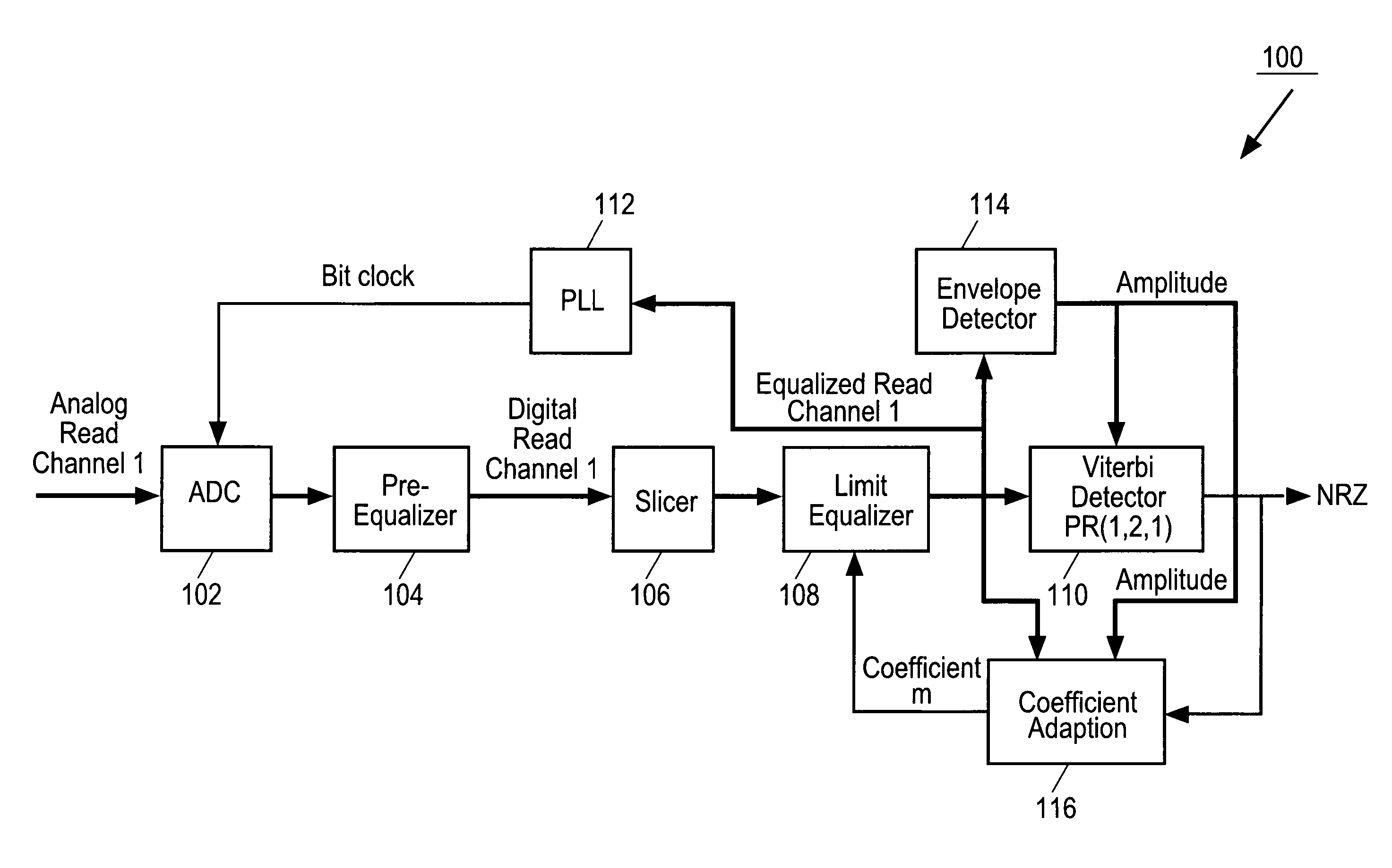
[0021]FIG. 1 is a block diagram of an embodiment of an electronic circuit of the invention,
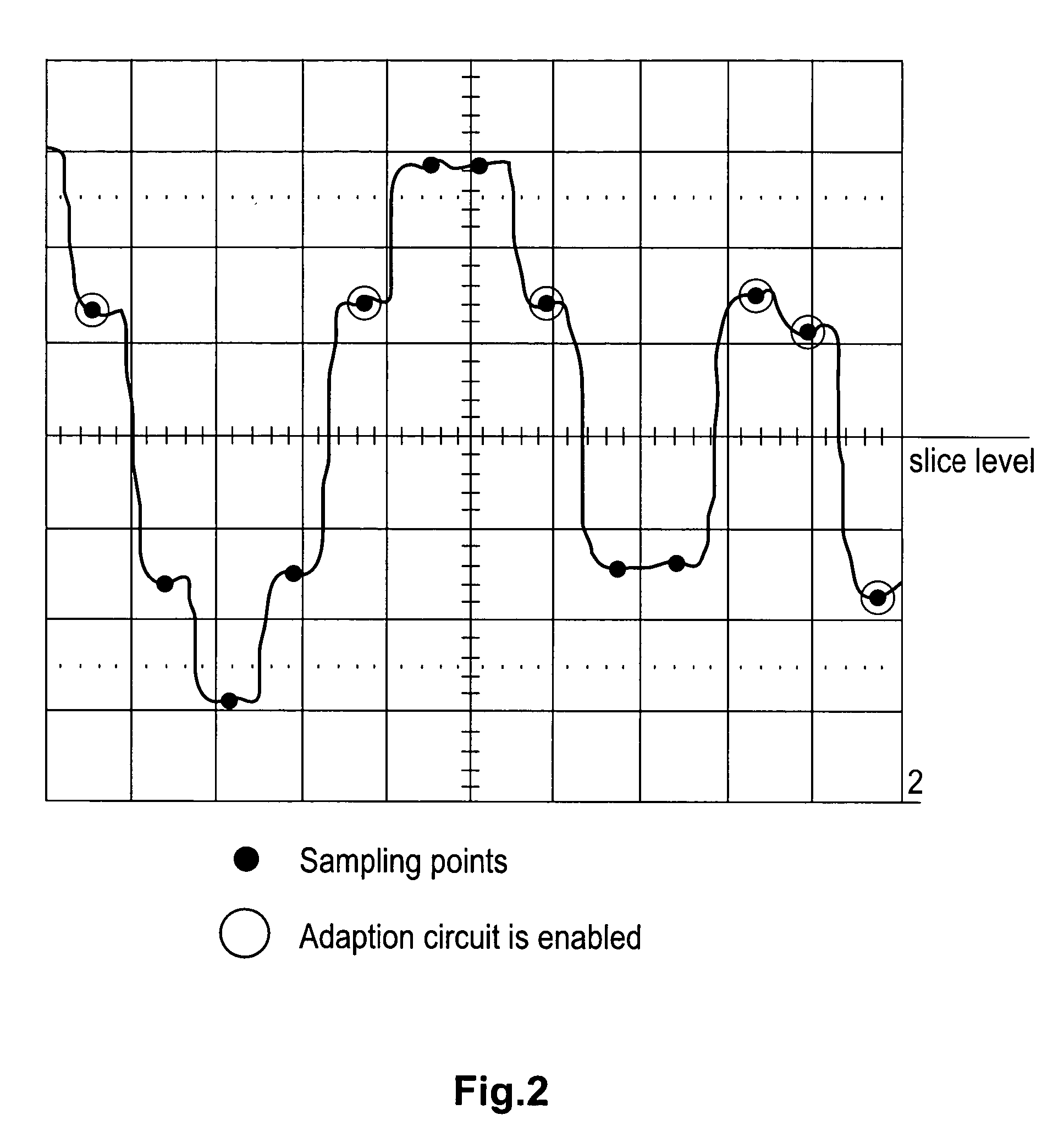
[0022]FIG. 2 shows the wave form at the output of the limit equalizer,
[0023]FIG. 3 shows the output of the limit equalizer measured with an DSO in persistence mode,
[0024]FIG. 4 shows the target waveform for the partial-response target PR(1,2,1), [0025]FIG. 5 shows a more detailed block diagram of the coefficient adaptation circuit module of FIG. 1,
[0026]FIG. 6 illustrates the timing detection for the half amplitude signal level,
[0027]FIG. 7 is illustrative of a flow chart of a method of the present invention.
DETAILED DESCRIPTION OF PREFERRED EMBODIMENTS
[0028]FIG. 1 shows a block diagram of electronic circuit 100 for decoding a read signal obtained from a high density optical disc. The electronic circuit 100 has analogue to digital converter (ADC...
PUM
 Abstract
Description
Claims
Application Information