Microfluidic assay devices

a microfluidic and assay technology, applied in the field of microfluidic assay devices, can solve the problems of inability to accurately detect the presence of microfluidic particles, etc., to achieve the effect of reducing the number of microfluidic particles

Inactive Publication Date: 2006-06-29
KIMBERLY-CLARK WORLDWIDE INC
View PDF57 Cites 33 Cited by
  • Summary
  • Abstract
  • Description
  • Claims
  • Application Information

AI Technical Summary

Problems solved by technology

Unfortunately, the use of active (or external) forces to induce flow is cost prohibitive and overly complex.
However, problems still exist with such conventi

Method used


Image

  • Microfluidic assay devices
  • Microfluidic assay devices
  • Microfluidic assay devices

Examples


example 1

[0058] The ability to form a microfluidic device in accordance with one embodiment of the present invention was demonstrated. Specifically, a micromolded polymer sheet was initially formed from polydimethylsiloxane (PDMS) silicone rubber (“Sylgard 184”, available from Dow Corning of Midland, Mich.). The PDMS prepolymer was a liquid having a viscosity of 3900 centipoise. The PDMS prepolymer was polymerized with a radical-mediated mechanism that employed a platinum-based catalyst (1 part catalyst: 10 parts prepolymer). The initial liquid properties of the PDMS allowed it to replicate finely structured molds with high fidelity and good dimensional stability.

[0059] A 50-micrometer thick photoresist (available from Dow Chemical under the name “EPON SU-8”) was then formed on a silicon wafer. Specifically, 3 milliliters of the SU-8 photoresist was dispensed at 100 RPM onto a 6″ diameter silicon wafer, ramped slowly to 500 RPM, and then ramped quickly to 2000 RPM and held for 30 seconds. T...

example 2

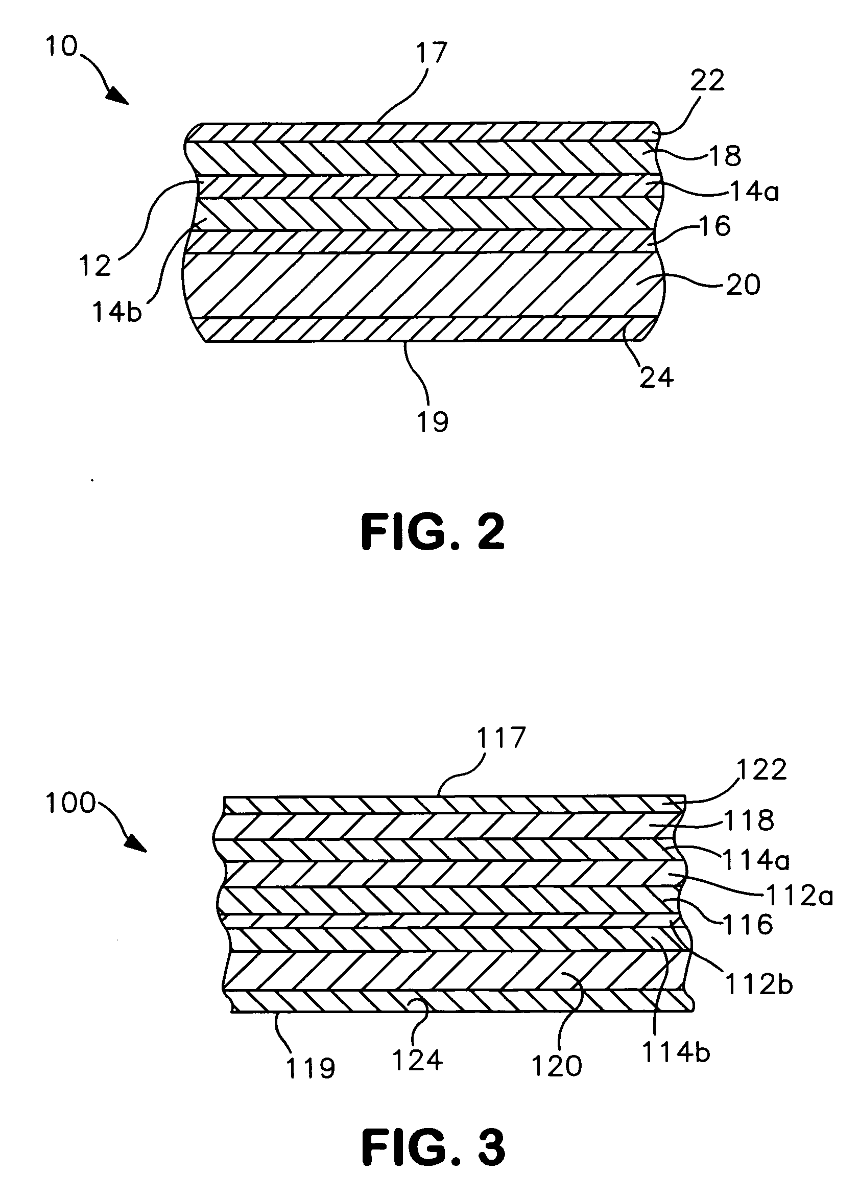
[0063] A microfluidic device was formed as described in Example 1, except that the design utilized is shown in FIG. 2 and had the following dimensions.

TABLE 2Dimensions of the Fluidic ZonesVolumeWidthDepthAspect(nanoliters)(micrometers)(micrometers)RatioInput Channel165400508Analysis Zone2603000 (max)5060Wicking45050501Channels(20×)Overflow Zone924022005044TOTAL10,115

example 3

[0064] A microfluidic device was formed as described in Example 1, except that the design utilized is shown in FIG. 3 and had the following dimensions.

TABLE 3Dimensions of the Fluidic ZonesVolumeWidthDepthAspect(nanoliters)(micrometers)(micrometers)RatioInput Channel165400508Analysis Zone2402000 (max)5050Wicking45050501Channels(20×)Overflow Zone924022005044TOTAL10,095


PUM


Abstract

A microfluidic assay device for determining the presence or absence of an analyte within a fluid test sample is provided. The present invention provides a technique for achieving continuous flow in a microfluidic device by using at least one input channel, an analysis zone, and a plurality of wicking channels disposed about the perimeter of the analysis zone. In one embodiment, for example, the wicking channels extend radially from the analysis zone. As a result of the particular configuration of the microfluidic device, an assay may performed in a “single step” without the need for active forces, such as a pressure source, electrokinetic force, etc., to induce flow of the fluid test sample through the device. Likewise, flow rate is controlled so that the dwell time of the fluid test sample within the analysis zone is long enough to allow for the desired reactions and/or detection.

Description

BACKGROUND OF THE INVENTION [0001] Microfluidic devices have been used in biochemical fields to perform high throughput screening assays. Microfluidic devices provide fluidic networks in which biochemical reactions, sample injections, and separation of reaction products may be achieved. In many conventional microfluidic devices, fluid flow and reagent mixing are achieved using electrokinetic transport phenomena (electroosmotic and electrophoretic). Electrokinetic transport is controlled by regulating the applied potentials at the terminus of each channel of the microfluidic device. Within the channel network, cross intersections and mixing tees are used for valving and dispensing fluids with high volumetric reproducibility. The mixing tee may be used to mix proportionately two fluid streams in ratio from 0 to 100% from either stream simply by varying the relative field strengths in the two channels. [0002] Unfortunately, the use of active (or external) forces to induce flow is cost ...

Claims


Application Information

Patent Timeline
IPC IPC(8): G01N33/20B01L3/00
CPCB01L3/502746B01L2300/069B01L2300/0803B01L2300/0816B01L2300/0864B01L2400/0406B01L3/00G01N35/00
Inventor COHEN, DAVID SAMUELFEASTER, SHAWN RAY
Owner KIMBERLY-CLARK WORLDWIDE INC
Why Eureka
Try Eureka