

Plasma processing apparatus with insulated gas inlet pore
- Summary
- Abstract
- Description
- Claims
- Application Information
AI Technical Summary
Benefits of technology
Problems solved by technology
Method used
Image

Examples
examples
[0051] The present invention will be explained with reference to the following examples. However, the examples are not intended to limit the present invention.
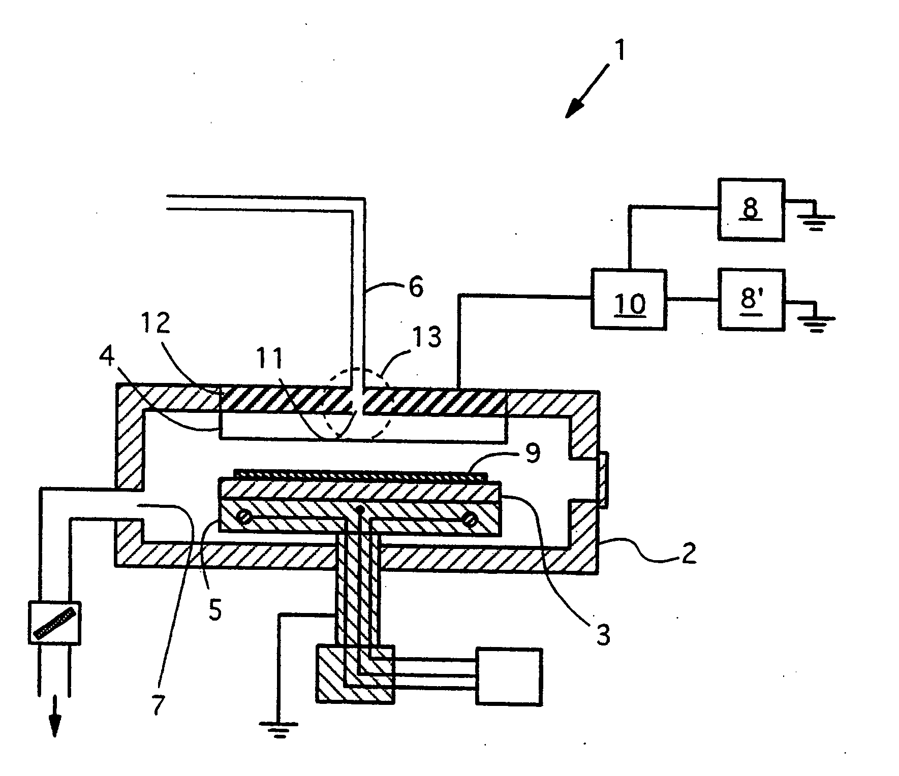
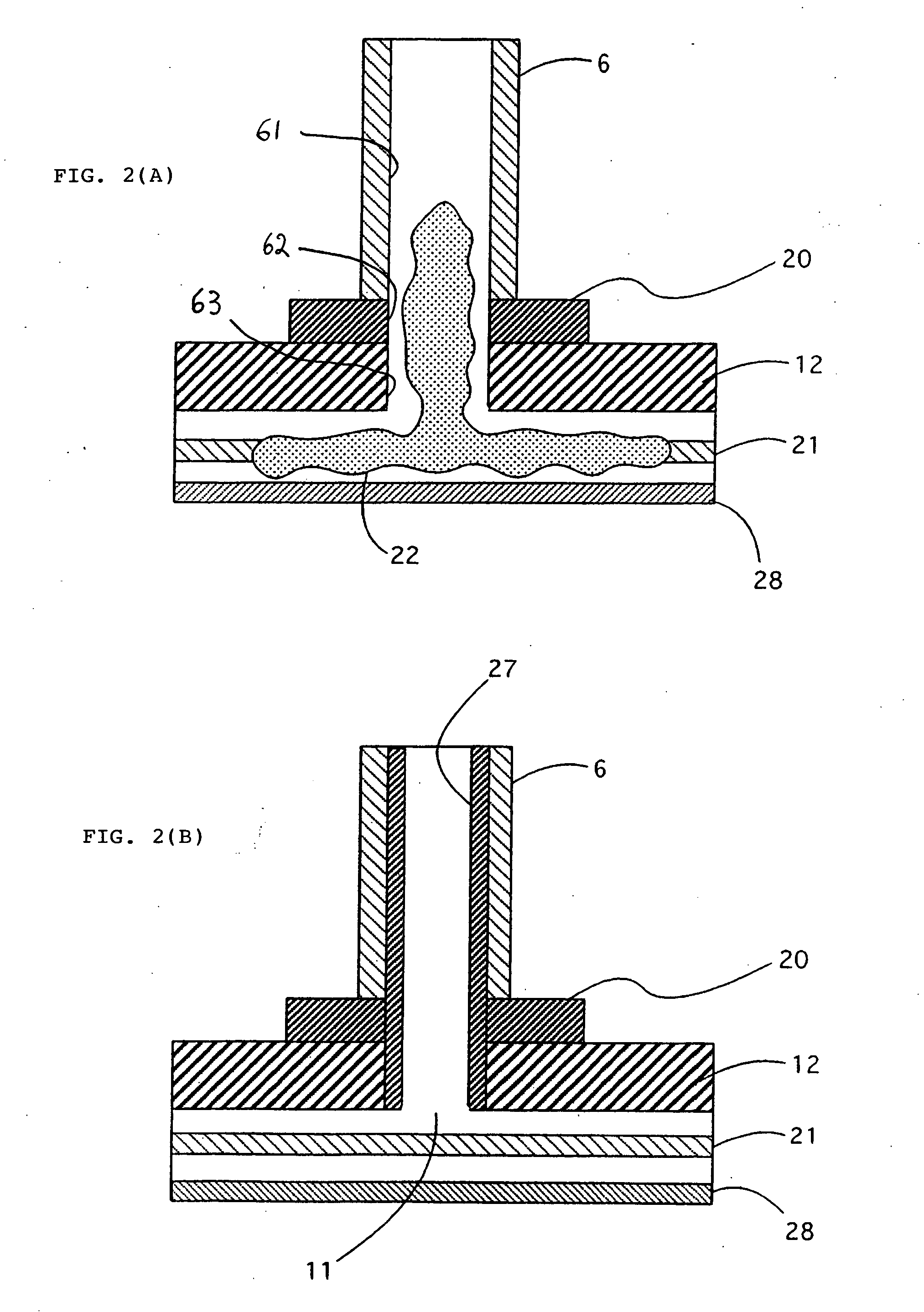
[0052] Thin-film formation experiments were conducted using a conventional plasma CVD apparatus and a plasma CVD apparatus according to an embodiment of the present invention (FIG. 2(B)). The tubular insulation was installed inside the a gas passage inner surface constituted by the inner wall 61 of the gas inlet piping 6, the inner periphery 62 of the ring-shaped insulator 20, and the inner periphery 63 of the gas inlet pore 11. The tubular insulator 27 had a radial thickness of 20 mm, an axial thickness (length) of 200 mm, and an inner diameter of 40 mm. In this case, the tubular insulator 27 covered a vertical portion of the gas inlet piping 6 in its entirety. The tubular insulator was made of aluminum oxide or magnesium oxide.
[0053] In the experiments, an oxygen-doped silicon carbide film and a nitrogen-doped silicon carb...
PUM
| Property | Measurement | Unit |
|---|---|---|
| Thickness | aaaaa | aaaaa |
| Electrical conductor | aaaaa | aaaaa |
| Electric potential / voltage | aaaaa | aaaaa |
Abstract
Description
Claims
Application Information