Semiconductor device and radio communication device

a technology of semiconductor devices and radio communication devices, applied in the direction of solid-state devices, transistors, basic electric elements, etc., can solve the problem of inability to prevent current localization, and achieve the effect of reducing the thermal resistance of semiconductor devices

Active Publication Date: 2006-06-29
MURATA MFG CO LTD
View PDF2 Cites 53 Cited by
  • Summary
  • Abstract
  • Description
  • Claims
  • Application Information

AI Technical Summary

Benefits of technology

[0012] In the case of adopting the semiconductor device having a layout in which thirty-six unit transistors Q′ are arranged as a matrix as shown in FIG. 33, when the semiconductor device is operated, the temperature of the inner portion of the substrate 104D viewed in the x-direction becomes higher than that of the outer portion thereof, as shown in FIG. 34, so that the unit transistors Q′ placed in the inner portion determine the disruptive strength and lifetime of the device. To reduce the temperature increase in the inner portion, it can be considered to enlarge the layout region by increasing the spacing between the unit transistors in the inner portion. However, the enlarged layout region mostly inhibits the miniaturization of the semiconductor device.
[0014] An object of the present invention is to provide a technology which allows a reduction in the thermal resistance of a semiconductor device and the miniaturization thereof.
[0015] Another object of the present invention is to provide a radio communication device using the miniaturized semiconductor device that has been reduced in thermal resistance.
[0021] There can be provided a technology which allows a reduction in the thermal resistance of a semiconductor device and the miniaturization thereof.

Problems solved by technology

Accordingly, it can be considered that a decrement in the base voltage of the unit transistor is small and therefore the current localization cannot be prevented.

Method used


Image

  • Semiconductor device and radio communication device
  • Semiconductor device and radio communication device
  • Semiconductor device and radio communication device

Examples


embodiment 1

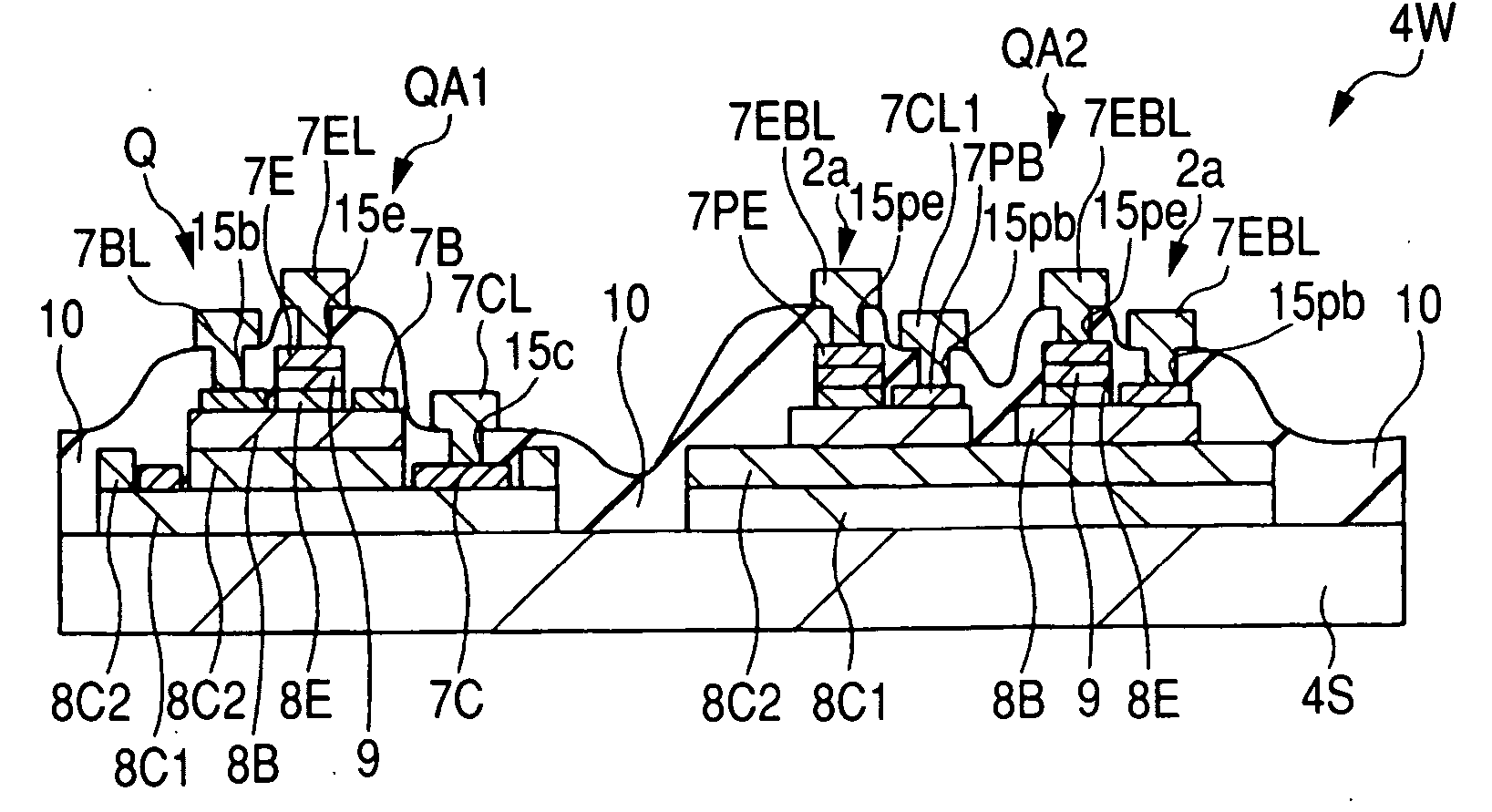
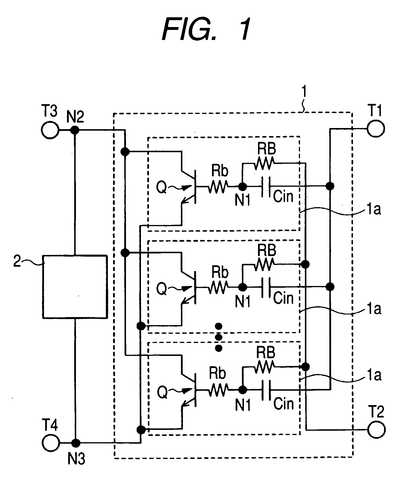
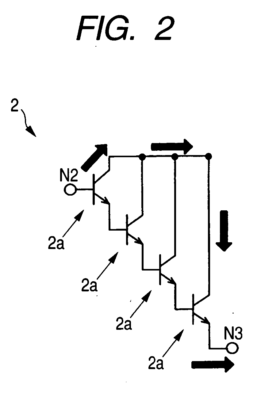
[0058] A semiconductor device shown in Embodiment 1 will be described with reference to FIGS. 1 to 13. The description will be given first to an amplifier circuit and a protective circuit in the semiconductor device shown in the present embodiment with reference to FIGS. 1 and 2, in which FIG. 1 is a circuit diagram of an amplifier circuit 1 and a protective circuit 2 in the semiconductor device shown in the present embodiment and FIG. 2 is a circuit diagram of the protective circuit 2 shown in FIG. 1.

[0059] As shown in FIG. 1, the amplifier circuit is constituted by a plurality of unit cells 1a connected in parallel. Each of the unit cells 1a is composed of a unit transistor Q which is, e.g., a hetero-junction bipolar transistor (hereinafter referred to as the HBT) and additional elements which are a base ballast resistor PB, a base resistor Rb, and a capacitor Cin.

[0060] The plurality of unit transistors Q have respective collectors coupled to each other, respective emitters cou...

embodiment 2

[0090] A semiconductor device shown in Embodiment 2 will be described with reference to FIGS. 14 and 15. In contrast to Embodiment 1 which has described the case where the HBT is used, the present embodiment will describe the case where a MOS (Metal Oxide Semiconductor) transistor is used.

[0091]FIG. 14 is a principal-portion schematic plan view of the semiconductor device shown in the present embodiment. FIG. 15 is a principal-portion schematic plan view of the semiconductor device taken along the line D2-D2 of FIG. 14.

[0092] As shown in FIG. 14, MOS transistors Qa and Qb, the pads BP, and wiring patterns 16 providing electrical connection therebetween have been laid out in the formation region 3 of the substrate 4S. The formation region 3 is provided with a plurality of transistor formation regions 3a and 3f having the MOS transistors Qa and a plurality of transistor formation regions 3b, 3c, 3d, and 3e having the MOS transistors Qb, which are arranged in the y-direction.

[0093] ...

embodiment 3

[0097] A semiconductor device shown in Embodiment 3 will be described with reference to FIGS. 16 to 24. The description will be given first to the amplifier circuit of the semiconductor device shown in the present embodiment with reference to FIG. 16. FIG. 16 is a circuit diagram of the amplifier circuit 1 shown in the present embodiment.

[0098] As shown in FIG. 16, the amplifier circuit 1 is composed of the plurality of unit transistors Q connected in parallel. The plurality of unit transistors Q have the respective collectors coupled to each other, the respective emitters coupled to each other, and the respective bases coupled to each other. As a result, the amplifier circuit is constituted to operate as though it is a single transistor with the common RF signal inputted to the input-side bases from the terminal T1. On the output side of the amplifier circuit 1, the unit transistors Q have the respective collectors connected commonly to the terminal T3 and the respective emitters ...


PUM


Abstract

A technology which allows a reduction in the thermal resistance of a semiconductor device and the miniaturization thereof is provided. The semiconductor device has a plurality of unit transistors Q, transistor formation regions 3a, 3b, and 3e each having a first number (seven) of the unit transistors Q, and transistor formation regions 3c and 3d each having a second number (four) of the unit transistors Q. The transistor formation regions 3c and 3d are located between the transistor formation regions 3a, 3b, 3e, and 3f and the first number is larger than the second number.

Description

CROSS-REFERENCE TO RELATED APPLICATION [0001] The present application claims priority from Japanese patent application No. 2004-379283 filed on Dec. 28, 2004, the content of which is hereby incorporated by reference into this application. BACKGROUND OF THE INVENTION [0002] The present invention relates to a semiconductor device. More particularly, it relates to a technology which is effective when applied to a semiconductor device having hetero-junction bipolar transistors (hereinafter referred to as HBTs) and to a radio communication device using the same. [0003] In a HBT using different semiconductor materials for an emitter and a base (e.g., AlGaAs / GaAs, InGaP / GaAs, or the like), a collector current can be increased without lowering a current amplification factor since the leakage of holes into the emitter is suppressed by the barrier of the emitter-base junction thereof. In addition, a reduction in the film thickness of the base layer reduces the transit time of electrons and th...

Claims


Application Information

Patent Timeline
Patent Type & Authority Applications(United States)
IPC IPC(8): H01L31/109
CPCH01L23/66H01L24/49H01L27/0605H01L29/7371H01L2223/6627H01L2223/6644H01L2224/48091H01L2224/48095H01L2224/48137H01L2224/48235H01L2224/49113H01L2224/49171H01L2924/01002H01L2924/01004H01L2924/01005H01L2924/01006H01L2924/01007H01L2924/01013H01L2924/01014H01L2924/01015H01L2924/0102H01L2924/01022H01L2924/01028H01L2924/01029H01L2924/01031H01L2924/01032H01L2924/01042H01L2924/01049H01L2924/01074H01L2924/01075H01L2924/01078H01L2924/01079H01L2924/01082H01L2924/10329H01L2924/10336H01L2924/14H01L2924/1423H01L2924/19032H01L2924/19041H01L2924/19042H01L2924/19043H01L2924/19105H01L2924/30105H01L2924/3011H01L24/48H01L2924/01033H01L2924/01037H01L2924/01041H01L2224/32225H01L2224/48227H01L2224/73265H01L28/40H01L29/0808H01L29/7304H01L27/067H01L2924/13091H01L2924/1305H01L2924/00014H01L2924/00H01L2224/05553H01L2924/30111H01L2224/45099H01L25/042
Inventor SASAKI, SATOSHIUMEMOTO, YASUNARIOSONE, YASUOKOBORI, TSUTOMUKUSANO, CHUSHIROOHBU, ISAOSASAKI, KENJI
Owner MURATA MFG CO LTD
Why Eureka
Try Eureka