Photoelectric Conversion Device and Method for Producing Photoelectric Conversion Device

a conversion device and photoelectric technology, applied in the direction of semiconductor devices, radio-controlled devices, electrical apparatus, etc., can solve the problems of remarkable problems and sensitivity lowering, and achieve the effect of reducing damage to the photoreceiving portion and damage, and increasing condensing efficiency

Inactive Publication Date: 2006-06-29
CANON KK
View PDF13 Cites 59 Cited by
  • Summary
  • Abstract
  • Description
  • Claims
  • Application Information

AI Technical Summary

Benefits of technology

[0016] A photoelectric conversion device having such a configuration can increase condensing efficiency because of having a large refraction index region on a photorece

Problems solved by technology

As a result, a photoelectric conversion device causes the lowering of its sensitivity.
Particularly when the photoelectric conversion device has taken a low F number (the aperture is fully opened),

Method used


Image

  • Photoelectric Conversion Device and Method for Producing Photoelectric Conversion Device
  • Photoelectric Conversion Device and Method for Producing Photoelectric Conversion Device
  • Photoelectric Conversion Device and Method for Producing Photoelectric Conversion Device

Examples


first embodiment

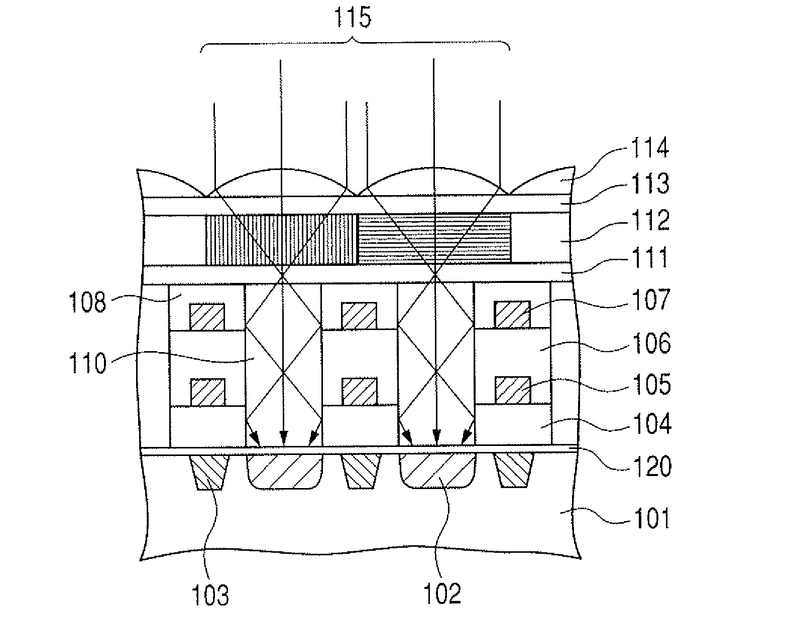
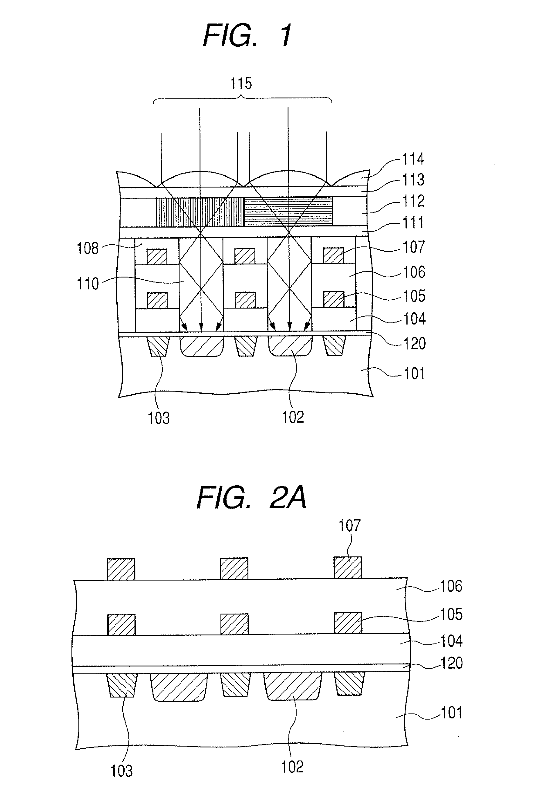
[0033] Embodiments according to the present invention will be now described with reference to the drawings. FIG. 1 is a typical sectional view showing one configuration example of a photoelectric conversion t device according to a

[0034] As is shown in FIG. 1, a photoelectric conversion device has a plurality of photoreceiving portions 102 formed at regions across a predetermined depth from the surface, in a semiconductor substrate 101; element isolation regions 103 provided in between the adjacent photoreceiving portions; an etching-stop layer 120 of a layer having a lower etching rate than an upper layer has, formed on the surface of a semiconductor substrate 101 so as to cover the whole surface of the photoreceiving portion 102; a first insulation film 104 provided on the etching-stop layer 120; and a transistor for transferring an electric charge formed around the surface of the semiconductor substrate 101, though it is not shown in the drawings. In the above configuration, the e...

second embodiment

[0064] In the next place, as a second embodiment, a photoelectric conversion device with no etching-stop layer 120 provided thereon will be described.

[0065]FIG. 3 is a typical sectional view showing one configuration example of a photoelectric conversion device according to a second embodiment. In FIG. 3, the same reference numeral as in FIG. 1 is attached for the same component as in the photoelectric conversion device shown FIG. 1, and a detailed description for the component is omitted. In addition, an element isolation region and a transistor for transferring an electric charge are not shown in the figure because of being the same as in a previous case.

[0066] A photoelectric conversion device shown in FIG. 3 has the first insulation film 125 formed on a semiconductor substrate 101 having a photoreceiving portion 102 formed therein; and sets the refractive index of the first insulation film 125 equal to that of a large refraction index region 110. In this case as well, the refra...

third embodiment

[0070] Now, as a third embodiment, a photoelectric conversion device having an etching-stop layer 120 arranged so as to cover one part of the gate electrode of a transistor for transferring an electric charge will be briefly described with reference to FIGS. 5A and 5B.

[0071] Both FIGS. 5A and 5B are typical sectional views showing one configuration example of a photoelectric conversion device, and showing the production steps therefor. In FIGS. 5A and 5B, the same reference numeral as in FIG. 1 is attached for the same component as in the photoelectric conversion device shown FIG. 1, and detailed description for the component is omitted.

[0072] In FIG. 5A, a gate electrode 140 of a transistor for transferring an electric charge is arranged in the vicinity of the surface of the semiconductor substrate 101, and of the diffusion region 150 of the transistor formed in the substrate. In addition, a contact portion 145 for electrical conduction is formed on the gate electrode 141 of anoth...


PUM


Abstract

A photoelectric conversion device according to the present invention has a plurality of photoreceiving portions provided in a substrate, an interlayer film overlying the photoreceiving portion, a large refraction index region which is provided so as to correspond to the photoreceiving portion and has a higher refractive index than the interlayer film, and a layer which is provided in between the photoreceiving portion and the large refraction index region, and has a lower etching rate than the interlayer film, wherein the layer of the lower etching rate is formed so as to cover at least the whole surface of the photoreceiving portion. In addition, the layer of the lower etching rate has a refractive index in between the refractive indices of the large refraction index region and the substrate. Such a configuration can provide the photoelectric conversion device which inhibits the lowering of the sensitivity and the variation of the sensitivity among picture elements.

Description

BACKGROUND OF THE INVENTION [0001] 1. Field of the Invention [0002] The present invention relates to a photoelectric conversion device used in a digital camera or the like, which forms an image by converting incident light to an electric charge. [0003] 2. Related Background Art [0004] For an image input device like a digital camera, a video camera and an image reader, a photoelectric conversion device is used such as a CCD (Charge Coupled Device) image sensor, or a non-CCD image sensor like a bipolar transistor image sensor, a field-effect transistor image sensor, a CMOS (Complementary Metal Oxide Semiconductor) image sensor and the like. The photoelectric conversion device converts optical image information to an electric signal, and the image input device processes these various converted electric signals to display them on a display for indication or record them in a storage medium. [0005] In order to acquire high performance, a photoelectric conversion device is desired to incre...

Claims


Application Information

Patent Timeline
IPC IPC(8): H01L31/0232
CPCH01L27/1462H01L27/14621H01L27/14625H01L31/02327H01L27/14629H01L27/14685H01L27/14627H01L27/14689H01L27/1463
Inventor HASHIMOTO, SAKAE
Owner CANON KK
Why Eureka
Try Eureka