Method for forming shallow trench isolation in semiconductor device

a technology of semiconductor devices and trenches, which is applied in the direction of semiconductor/solid-state device manufacturing, basic electric elements, electric apparatus, etc., can solve the problems of reducing the threshold voltage of transistors, affecting the formation of integrated circuits, and damage to silicon substrates, so as to improve the profile of semiconductor substrates, prevent oxide thinning, and improve transistor performance

Inactive Publication Date: 2006-06-29
DONGBU ELECTRONICS CO LTD
View PDF5 Cites 18 Cited by
  • Summary
  • Abstract
  • Description
  • Claims
  • Application Information

AI Technical Summary

Benefits of technology

[0014] It is, therefore, an object of the present invention to provide a method for improving the profile of the semiconductor substrate in the vicinity of top corners of the isolation trench. The electric field concentration and silicon lattice damage in the vicinity of top corners of the isolation trench can be effectively prevented. In addition, the present invention can prevent the oxide thinning at top corners of the isolation trench. Thus, the present invention can improve the performance of transistors, particularly high voltage transistors with thick gate oxide dimensions.

Problems solved by technology

However, due to the increase of the integration density, a LOCOS field oxide has become disadvantageous to the formation of integrated circuits, because it generally includes a “bird's beak,” which may invade an active device region.
The formation of the trench oxide generally involves a high-temperature heat treatment that may produce or result in damage to the silicon substrate.
This oxide thinning at the upper corner of the trench may result in degradation of the threshold voltage of the transistor.
As a result, the performance of the transistor may be deteriorated.

Method used


Image

  • Method for forming shallow trench isolation in semiconductor device
  • Method for forming shallow trench isolation in semiconductor device
  • Method for forming shallow trench isolation in semiconductor device

Examples


Embodiment Construction

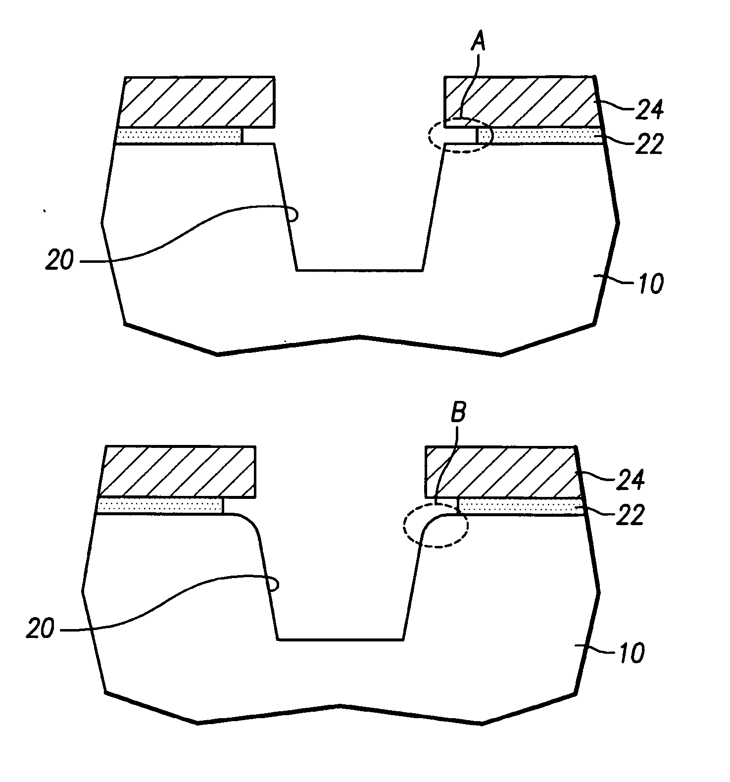
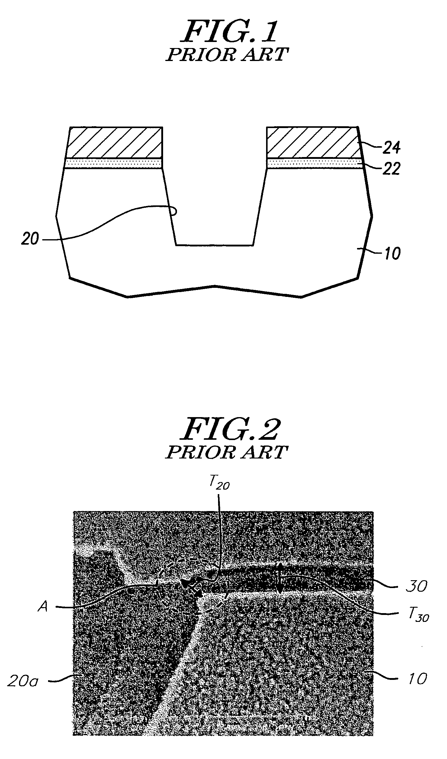
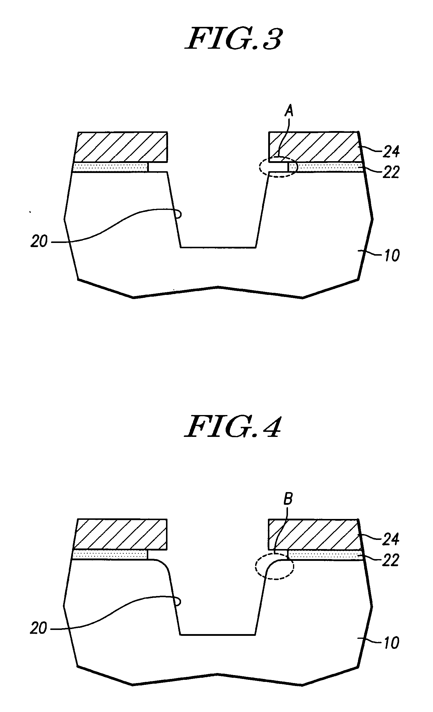
[0022] In FIGS. 3 and 4, the illustrated trench structure has a bird's beak shape at upper corners of the trench 20, which can be formed in such a manner as described hereinafter.

[0023] First, a pad oxide 22 and pad nitride 24 are formed on a silicon substrate 10 in successive order. Next, a photoresist pattern (now shown) is formed on the pad nitride 24 by a photolithography process. The photoresist pattern defines an opening over an isolation region in which a trench structure 20 is be formed. The opening exposes a portion of a top surface of the pad nitride 24 disposed over the isolation region.

[0024] After definition of the photoresist pattern, the portion of the pad nitride 24 exposed by the opening of the photoresist pattern is removed, exposing a portion of the pad oxide 22. The exposed portion of the pad oxide 22 is then removed, exposing a top surface of the substrate 10. Continuously, the exposed isolation region of the substrate 10 is etched in a predetermined depth, so...


PUM


Abstract

A method for forming shallow trench isolation in a semiconductor device. The method includes forming a pad oxide and a pad nitride on a semiconductor substrate in successive order, forming a trench in the substrate by etching the pad nitride, the pad oxide and the substrate, removing a portion of the pad oxide to expose top corners of the trench, and rounding the exposed portion of the top corners of the trench by a wet chemical etch.

Description

[0001] This application claims the benefit of Korean Application No. 10-2004-0115783, filed on Dec. 29, 2004, which is incorporated by reference herein in its entirety. BACKGROUND OF THE INVENTION [0002] 1. Field of the Invention [0003] The present invention relates generally to a semiconductor device manufacturing technology, and particularly to a method for forming shallow trench isolation in a semiconductor device. [0004] 2. Description of the Related Art [0005] Manufacturing processes for making highly integrated semiconductor devices involve forming a variety of components, such as a transistor, capacitor, metal wiring, etc., in very restricted regions, and forming highly insulated regions to prevent parasitic current leakage between the components. [0006] Conventionally, a local oxidation of silicon (LOCOS) field oxide, formed by oxidizing a silicon substrate, has been widely used for isolating the components of the semiconductor device. However, due to the increase of the int...

Claims


Application Information

Patent Timeline
Patent Type & Authority Applications(United States)
IPC IPC(8): H01L21/20
CPCH01L21/76232
Inventor KIM, JUNG HO
Owner DONGBU ELECTRONICS CO LTD
Why Eureka
Try Eureka