Circuit simulation method and circuit simulation apparatus

a circuit simulation and circuit simulation technology, applied in the field of circuit simulation methods and circuit simulation apparatuses, can solve the problems of reducing the simulation precision of circuit simulators, affecting the simulation accuracy of circuit simulators, so as to achieve the effect of improving the simulation precision

Inactive Publication Date: 2006-06-29
PANASONIC CORP
View PDF15 Cites 51 Cited by
  • Summary
  • Abstract
  • Description
  • Claims
  • Application Information

AI Technical Summary

Benefits of technology

[0016] The present invention has an object to provide a method capable of forming a transistor model in high precision with respect to widths of element isolating-purpose insulating films over a wide range by using a continuous mathematical model based upon such a transistor model having a parameter which has been fitted by a predetermined element isolating-purpose isolating film width.
[0020] In the circuit simulation method and circuit simulation apparatus of the present invention, the approximate expression as to the isolation width depending parameter is arranged by containing a polynomial of an inverse number of the isolation width parameter, and also, another polynomial having a depending characteristic as to both a channel width and a channel length of the transistor, so that as isolation width depending parameter can be obtained in high precision.
[0024] In accordance with the present invention, based upon the transistor model, the approximate expression of the parameter having the element isolating-purpose insulating film width depending characteristic is formed, and the value of the corrected parameter obtained by employing the formed approximate expression is replaced by the value of the original parameter, so that the transistor model of such a transistor is formed in which the element isolating-purpose insulating film widths are different from each other. As a result, such a transistor model which can be fitted to the drain current characteristic of the desirable isolation width can be easily formed. As a consequence, the circuit simulation can be carried out while considering the depending characteristic of the element isolating-purpose insulating film which constitutes the index of the stress, and thus, the simulation precision can be improved.

Problems solved by technology

In particular, in transistors using such element isolation techniques as STI (Shallow Trench Isolation) and the like, a specific attention has been paid to such a fact that the below-mentioned phenomenon may constitute a factor which impede an improvement in simulation precision of circuit simulators.
However, a lengthy time is required even when the reference table itself is formed, and further, very cumbersome processing steps are required, namely, when the optimum transistor model is selected from the plural transistor models, the transistor size data extracted from the circuit layout data to be simulated must be compared with the information stored in the reference table, so that mistakes caused by man may be easily made.
As a result, there is a risk that the simulating precision is lowered.
However, the resulting circuit simulating method may be cumbersome, for instance, necessities of increasing a total condition number as to the element isolating-purpose insulating film widths of the measuring-purpose devices must be increased; a cumbersome operation is necessarily required so as to recognize the shapes of the transistors; and a cumbersome operation is necessarily required in order to select the proper transistor model.
As a consequence, there is a limitation in the total quantity of the transistor models.

Method used


Image

  • Circuit simulation method and circuit simulation apparatus
  • Circuit simulation method and circuit simulation apparatus
  • Circuit simulation method and circuit simulation apparatus

Examples


embodiment mode 1

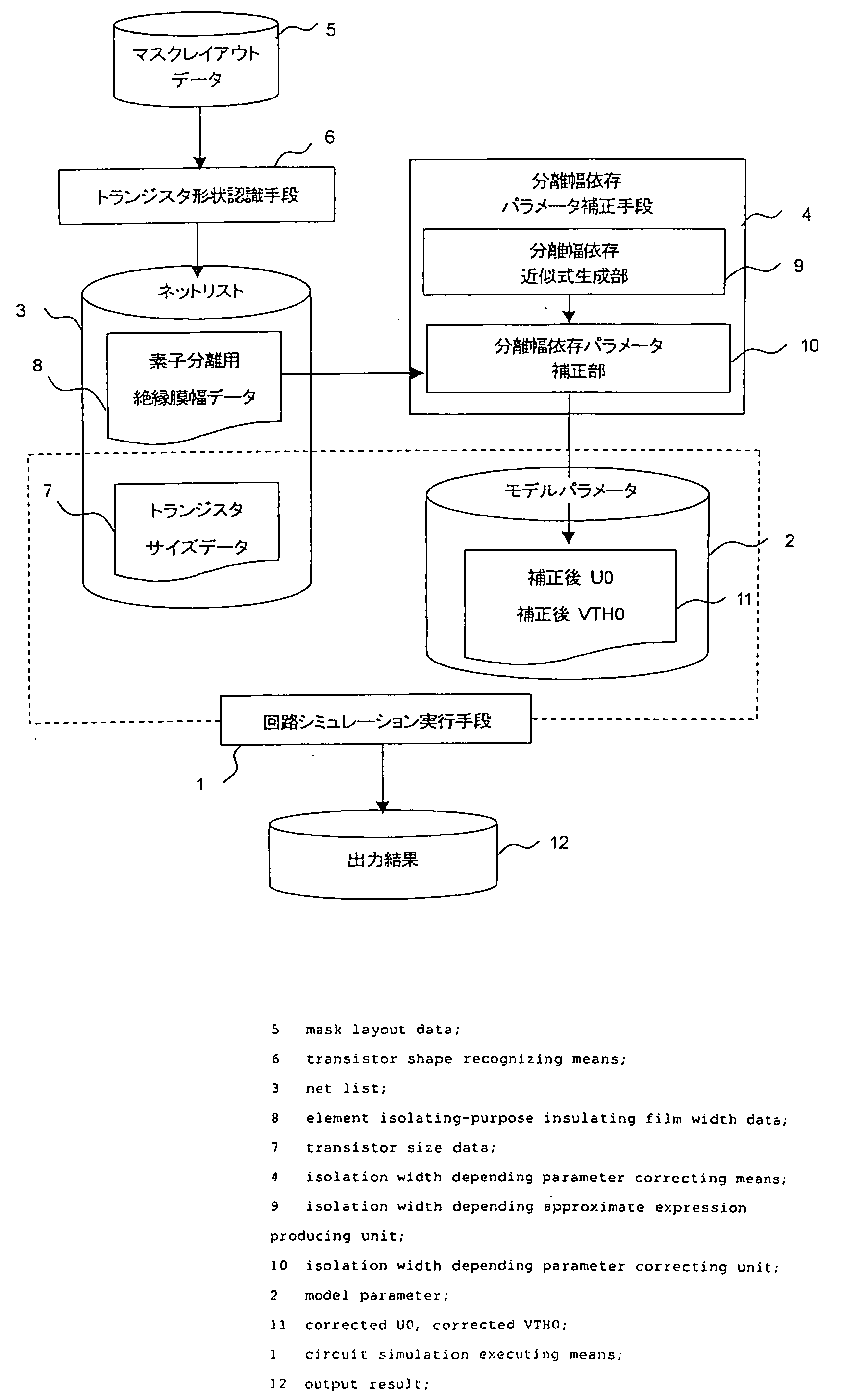
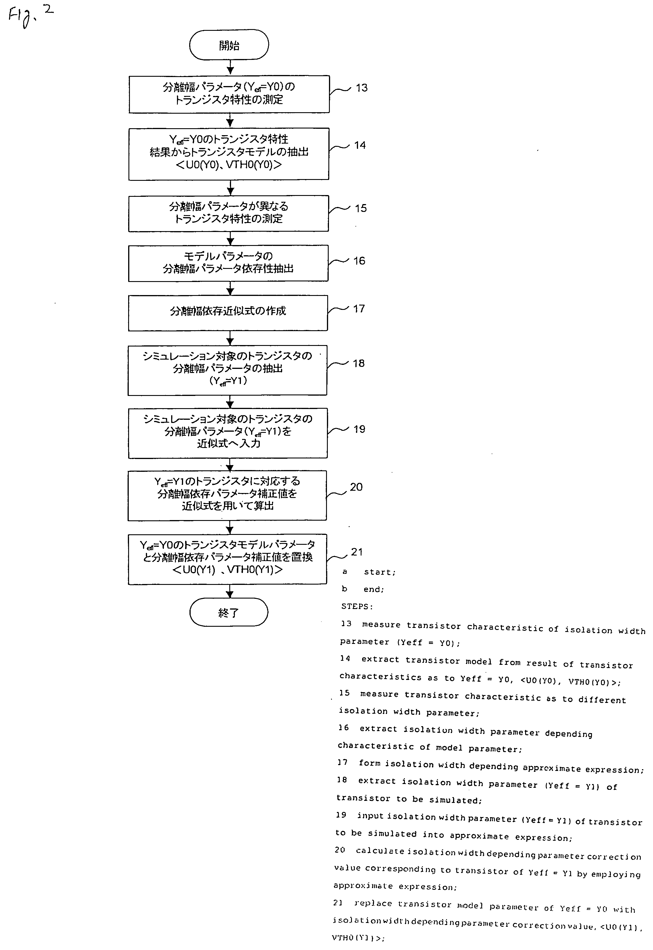
[0036]FIG. 1 is a block diagram for indicating an arrangement of a circuit simulation apparatus according to an embodiment mode 1 of the present invention.

[0037] A circuit simulation executing means 1 corresponds to a main body of a circuit simulator is typically known as SPICE (Software Process Improvement and Capability dEtermination) similar to the prior art, and corresponds to a circuit simulation executing program operated on a computer. A net list 3 and a model parameter 2 are entered to the circuit simulation executing means 1 so as to calculate an electric characteristic of a circuit which should be simulated, which is similar to that of the prior art. The net list 3 has been extracted from mask layout data of the circuit which should be simulated. The model parameter 2 has been extracted from an actually measured value of a device characteristic. However, this circuit simulation apparatus owns such a novel point that an isolation width depending parameter correcting means ...

embodiment mode 2

[0056]FIG. 6(a) is a plan view for indicating an example of a transistor according to an embodiment mode 2 of the present invention. It should be understood that the same reference numerals shown in the embodiment mode 1 will be employed as those for denoting the same, or similar structural elements of the embodiment mode 2. A different point between the modeling method of this embodiment mode 2 and the embodiment mode 1 is given as follows: That is, as indicated in FIG. 6(a), a modeling method can be carried out in such a case that shapes of activated regions 24 adjacent to each other along a width direction of a channel of the transistor are irregular.

[0057] In FIG. 6(a), regions of element isolating-purpose insulating films where an influence of a stress given to the channel of the transistor is expected to be especially strong are defined as a useful element isolating-purpose insulating film region 25a and another useful element isolating-purpose insulating film region 25b. The...

embodiment mode 3

[0061]FIG. 7 is a plan view for indicating an example of a transistor according to an embodiment mode 3 of the present invention. It should be understood that the same reference numerals shown in the embodiment mode 1 will be employed as those for denoting the same, or similar structural elements of the embodiment mode 3. A different point between the modeling method of this embodiment mode 3 and the embodiment mode 1 is given as follows: That is, as indicated in FIG. 7, a modeling method can be carried out in such a case that shapes of activated regions 24 adjacent to each other along a width direction of a channel of the transistor are irregular.

[0062] As shown in FIG. 7, a straight line 27 is defined, while this straight line 27 is originated from a cross point “P” between an activated region 22 of a transistor and a center line 26 of a gate thereof up to a point “P′” of an edge of another activated region 24 which is located adjacent to the first-mentioned activated region 22 a...


PUM


Abstract

A circuit simulation apparatus and a modeling method are provided which are useful to design an integrated circuit in a very fine manner by forming a model of such a transistor that widths of element isolating-purpose insulating films are different from each other. In an isolation width depending parameter correcting means 4 of the present invention, an approximate expression of a parameter having an element isolating-purpose insulating film width depending characteristic is formed, and a value of a corrected parameter obtained by employing the formed approximate expression is replaced by a value of an original parameter, so that a transistor model of such a transistor is formed in which element isolating-purpose insulating film widths are different from each other. As a consequence, circuit simulation can be carried out in high precision by considering a change in transistor characteristics caused by a stress, which are approximated to actually measured data.

Description

BACKGROUND OF THE INVENTION [0001] 1. Field of the Invention [0002] The present invention relates to a circuit simulation method and a circuit simulation apparatus. More specifically, the present invention is directed to a modeling method of an integrated circuit, in particular, a circuit simulation apparatus which is used to design integrated circuits in high precision. [0003] 2. Description of the Related Art [0004] Very recently, while system LSIs and the like are developed, strong demands are made of further improving simulation precision of circuit simulators. More specifically, in connection with great progress as to very fine processing techniques of semiconductors, layout patterns and arrangements of circuit elements may give large influences to performance of circuits. In particular, in transistors using such element isolation techniques as STI (Shallow Trench Isolation) and the like, a specific attention has been paid to such a fact that the below-mentioned phenomenon may ...

Claims


Application Information

Patent Timeline
Patent Type & Authority Applications(United States)
IPC IPC(8): G06F17/50
CPCG06F17/5036G06F30/367
Inventor ISHIZU, TOMOYUKIUMEDA, TAKUYAOOTANI, KATSUHIROSAHARA, YASUYUKI
Owner PANASONIC CORP
Why Eureka
Try Eureka