Eureka AIR delivers breakthrough ideas for toughest innovation challenges, trusted by R&D personnel around the world.

CMOS image sensor and method for manufacturing the same

a technology of image sensor and manufacturing method, which is applied in the field of cmos image sensor, can solve the problems of limited light-receiving area of photodiodes, and inability to form metal lines over photodiodes, etc., and achieve the effect of improving light-receiving efficiency

Active Publication Date: 2006-07-06
III HLDG 4
View PDF9 Cites 9 Cited by
  • Summary
  • Abstract
  • Description
  • Claims
  • Application Information

AI Technical Summary

Benefits of technology

[0036] An advantage of the present invention is to provide a CMOS image sensor, and a method for manufacturing the same, that improves light-receiving efficiency.
[0037] Another advantage of the present invention is to provide a CMOS image sensor, and a method for manufacturing the same, that maintains a margin in the design of a metal line.

Problems solved by technology

As a result, the size of the light-receiving area for the photodiode is restricted.
Also, it is impossible to form the metal line over the photodiode.
Accordingly, the design of the metal line is restricted.

Method used


Image

  • CMOS image sensor and method for manufacturing the same
  • CMOS image sensor and method for manufacturing the same
  • CMOS image sensor and method for manufacturing the same

Examples


Embodiment Construction

[0056] Reference will now be made in detail to exemplary embodiments of the present invention, examples of which are illustrated in the accompanying drawings. Wherever possible, the same reference numbers will be used throughout the drawings to refer to the same or similar parts.

[0057] A CMOS image sensor and a method for manufacturing the same according to the present invention will be described with reference to the accompanying drawings.

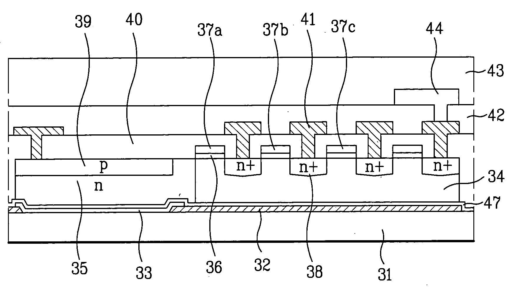
[0058]FIG. 6 is a cross sectional view of a CMOS image sensor according to an exemplary embodiment of the present invention. The CMOS image sensor includes an active area and a field area, wherein the active area includes a photodiode region and a transistor region.

[0059] As shown in FIG. 6, a black matrix layer 32 is formed on a transparent substrate, such as a glass substrate or a quartz substrate, 31 corresponding to the field area and the active area excluding the photodiode region. The black matrix layer 32 may be formed of a metal materia...


PUM


Abstract

A CMOS image sensor and a method for manufacturing the same improve light-receiving efficiency and maintain a margin in the design of a metal line. The CMOS image sensor includes a transparent substrate including an active area having a photodiode region and a transistor region and a field area for isolation of the active area, a p-type semiconductor layer on the transparent substrate, a photodiode in the p-type semiconductor layer corresponding to the photodiodes region, and a plurality of transistors in the p-type semiconductor layer corresponding to the transistor region.

Description

[0001] This application claims the benefit of Korean Patent Application No. 10-2004-0116482 filed on Dec. 30, 2004, and Korean Patent Application No. 10-2005-0120283 filed on Dec. 9, 2005, which is hereby incorporated by reference for all purposes as if fully set forth herein. BACKGROUND OF THE INVENTION [0002] 1. Field of the Invention [0003] The present invention relates to a CMOS image sensor, and a method for manufacturing the same, that improves the light-receiving efficiency of a photodiode. [0004] 2. Discussion of the Related Art [0005] An image sensor is a semiconductor device that converts an optical image to an electric signal. Image sensors can be broadly categorized into charge coupled devices (CCD) and complementary metal oxide semiconductor (CMOS) image sensors. [0006] In a CCD, respective metal-oxide-silicon MOS capacitors are positioned adjacently, wherein electric charge carriers are stored in and transferred to the capacitors. However, a CMOS image sensor adopts CM...

Claims


Application Information

Patent Timeline
Patent Type & Authority Applications(United States)
IPC IPC(8): H01L31/113H01L27/14H01L27/146H04N25/00
CPCH01L27/14621H01L27/14623H01L27/14685
Inventor HA, HYEON WOO
Owner III HLDG 4
Why Eureka
Eureka Blog
Learn More