Sonos device and method of manufacturing the same

Active Publication Date: 2006-07-06
MARVELL ASIA PTE LTD +1
View PDF4 Cites 7 Cited by
  • Summary
  • Abstract
  • Description
  • Claims
  • Application Information

AI Technical Summary

Benefits of technology

[0012] One advantage of the present invention is that it can prevent rupture of an ONO structure used as a charge trap layer.
[0013] An exemplary SONOS device according to an embodiment of the present invention includes: a source and a drain formed with a channel therebetween on a semiconductor substrate; a tunnel dielectric layer formed on the semiconductor substrate; a charge trap layer formed on the tunnel dielectric layer; a charge blocking layer formed on the charge trap layer such that the charge blocking layer is relatively thicker at regions adjacent to or overlapping the source and the drain and is relatively thinner at a region overlapping the channel between the relatively thicker regions; and a gate formed on the charge blocking layer.
[0014] The tunnel dielectric layer may include a silicon oxide layer, the charge trap layer may include a silicon nitride layer, and the charge blocking layer may include a silicon oxide layer.
[0015] An exemplary method of manufacturing a SONOS device according to an embodiment of the present invention includes: forming a tunnel dielectric layer on a semiconductor substrate; forming a charge trap layer on the tunnel dielectric layer; forming a charge blocking layer on the charge trap layer such that the charge blocking layer is relatively thicker at regions adjacent to or overlapping source and drain regions and is relatively thinner at a region overlapping a channel region between the source and drain regions; and forming a gate on the charge blocking layer.
[0016] Formation of the charge blocking layer may include: forming a first charge blocking layer on the charge trap layer; selectively etching a region of the first charge blocking layer overlapping the channel; forming a second charge blocking layer on the etched first charge blocking layer, the second blocking layer having locally thicker regions where the steps are formed by the etching of the first charge blocking layer; and patterning the second charge blocking layer such that the locally thicker regions may be adjacent to or overlap the source and the drain.
[0017] Selectively etching the first charge blocking layer may include: forming a mask exposing the region of the first charge blocking layer overlapping the channel; and selectively etching the first charge blocking layer exposed by the mask, such that the lower charge trap layer is exposed.

Problems solved by technology

However, one significant problem with this type of devices is that for write and erase operations they require application of a high voltage that may ultimately destroy the ONO layer with the charge trap layer.
This causes the overlap region to become unnecessarily charged with electrons.

Method used


Image

  • Sonos device and method of manufacturing the same
  • Sonos device and method of manufacturing the same
  • Sonos device and method of manufacturing the same

Examples


Embodiment Construction

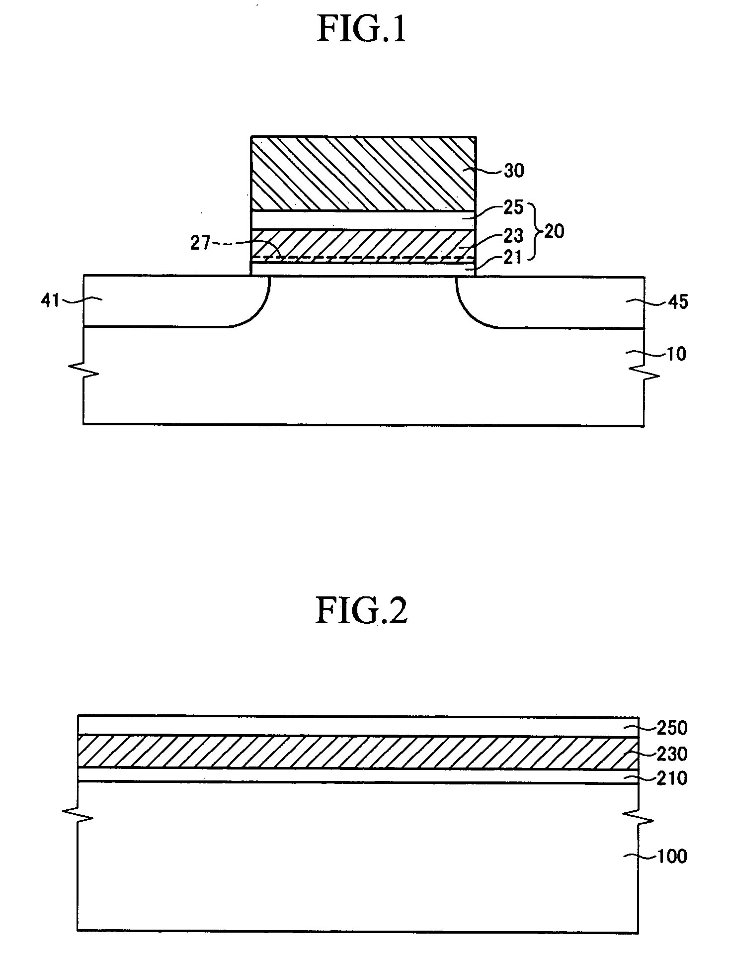
[0024] Reference will now be made in detail to an exemplary embodiment of the present invention, examples of which are illustrated in the accompanying drawings.

[0025] In an exemplary embodiment of the present invention, a method for locally thickening the region of an ONO structure in which a gate is overlapped with a source and a drain is provided. In this exemplary embodiment, rupture characteristics of the ONO structure may be improved.

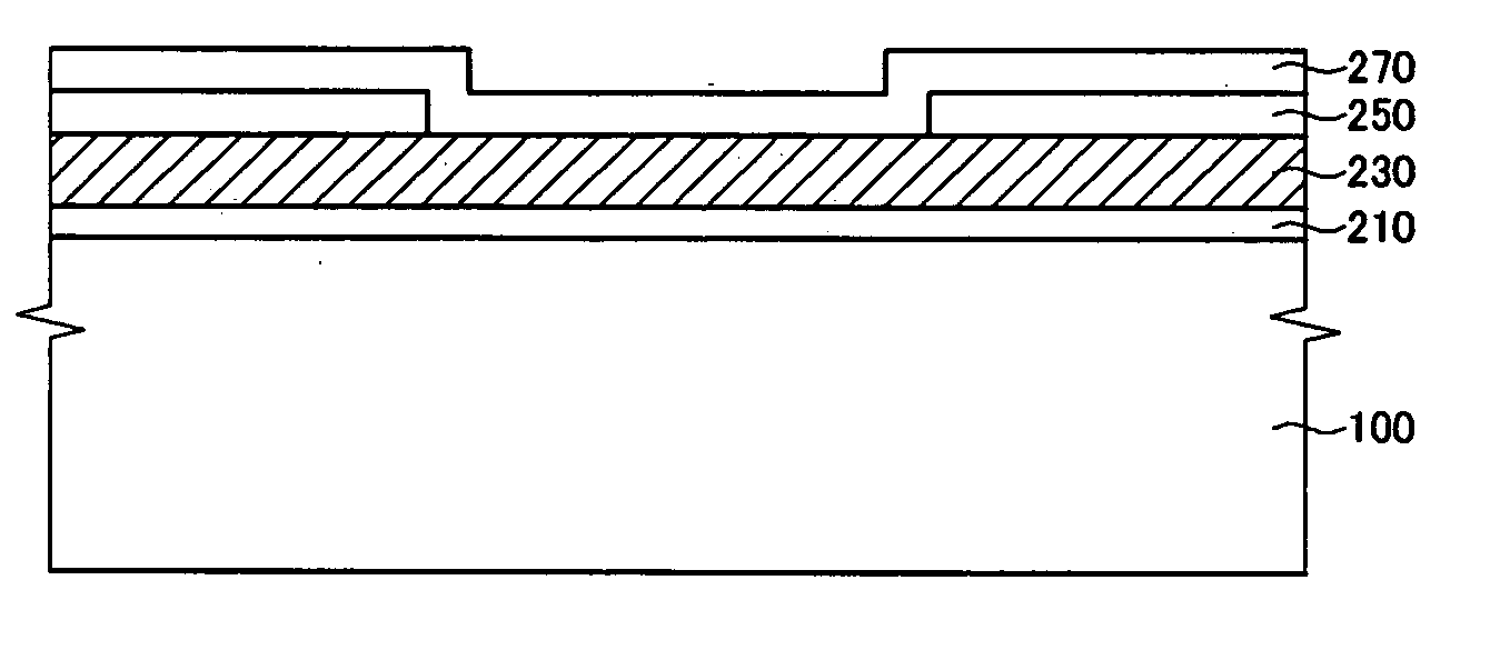
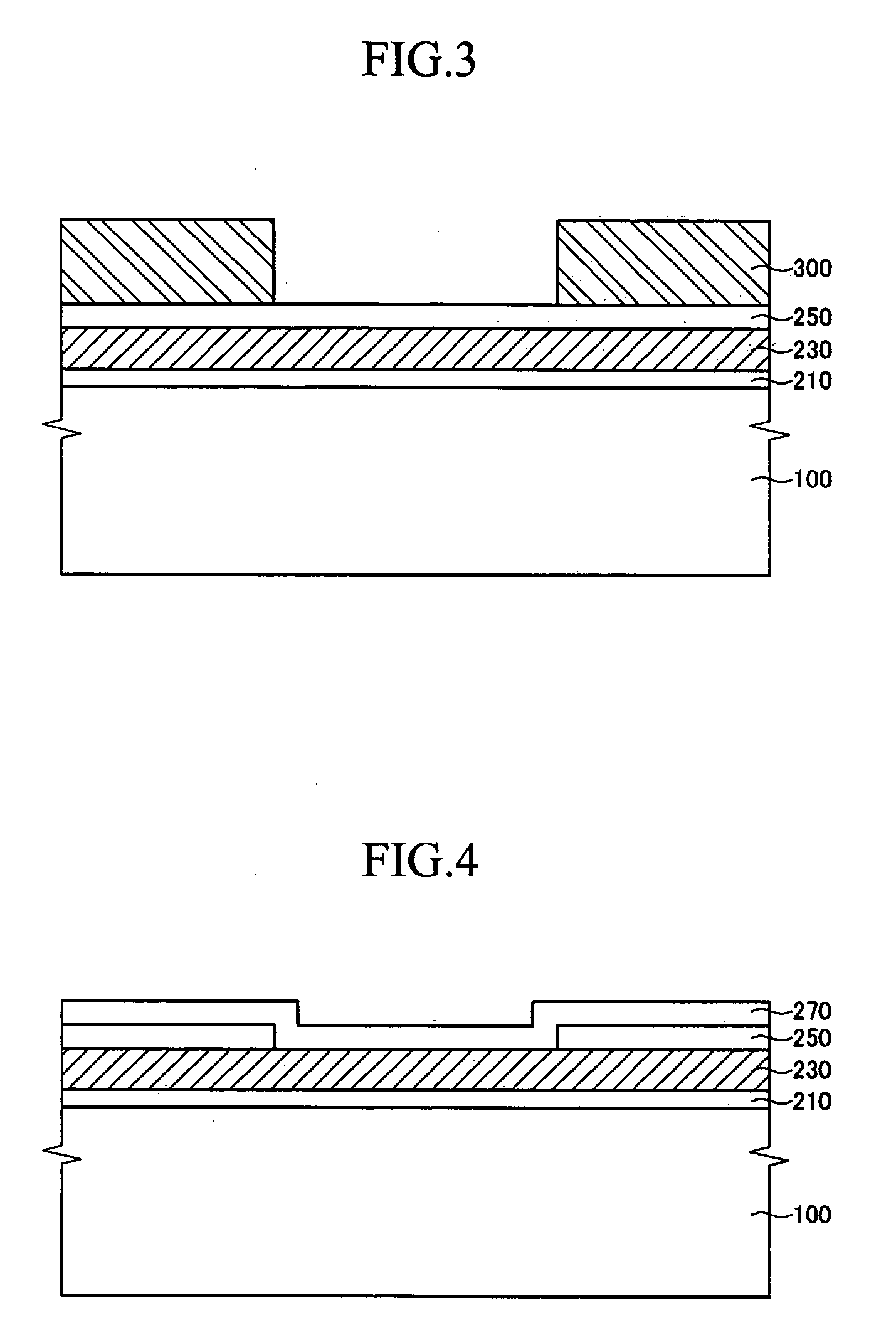
[0026] According to an embodiment of the present invention, an ONO layer is deposited, and then a part of a region of the uppermost oxide layer is removed. Another oxide layer is then separately deposited thereon to form an uppermost oxide layer. Therefore, the thickness of the portion of the ONO structure overlapping with the channel region can remain the same as in a conventional device; however, the thickness of the portion of the ONO structure overlapping or adjacent to the source and the drain is relatively larger.

[0027] When the SONOS tran...


PUM


Abstract

A SONOS device and a method of manufacturing the same is provided. A tunnel dielectric layer, a charge trap layer, and a charge blocking layer are formed on a semiconductor substrate, and the charge blocking layer is formed on the charge trap layer such that the charge blocking layer is relatively thicker at regions adjacent to or overlapping the source and the drain and relatively thinner at a region overlapping the channel region. A gate is then formed on the blocking layer.

Description

CROSS-REFERENCE TO RELATED APPLICATION [0001] This application claims priority to and the benefit of Korean Patent Application No. 10-2004-0117148 filed in the Korean Intellectual Property Office on Dec. 30, 2004, the entire contents of which are incorporated herein by reference. BACKGROUND OF THE INVENTION [0002] 1. Field of the Invention [0003] The present invention relates to a semiconductor device. More particularly, the present invention relates to a Silicon-Oxide-Nitride-Oxide-Silicon (SONOS) device in which protection from rupture of an Oxide-Nitride-Oxide (ONO) layer with a charge trap layer is enhanced, and a method of manufacturing the same. [0004] 2. Description of the Related Art [0005] SONOS devices are considered to be very important as non-volatile memory devices. However, one significant problem with this type of devices is that for write and erase operations they require application of a high voltage that may ultimately destroy the ONO layer with the charge trap lay...

Claims


Application Information

Patent Timeline
IPC IPC(8): H01L29/788
CPCH01L21/28282H01L29/42364H01L29/792H01L29/40117H01L21/3105H01L29/66833
Inventor KWON, SUNG-WOO
Owner MARVELL ASIA PTE LTD
Why Eureka
Try Eureka