Semiconductor device having vertical metal insulator semiconductor transistors having plural spatially overlapping regions of different conductivity type

a technology of vertical metal insulator and semiconductor transistor, which is applied in the direction of semiconductor devices, semiconductor/solid-state device details, electrical equipment, etc., can solve the problems of reducing on resistance, forming fine structures, and depleting the pillar layers

Inactive Publication Date: 2006-07-06
OKUMURA HIDEKI +6
View PDF16 Cites 9 Cited by
  • Summary
  • Abstract
  • Description
  • Claims
  • Application Information

AI Technical Summary

Problems solved by technology

However, this patent does not clearly state that it can completely deplete the pillar layers and reduce the on resistance.
Thus, this patent fails to form a fine structure in a substrate planar direction and thus does not serve to reduce the on resistance.
As a result, the number of epitaxial growth layers (102a to 102k) increases as shown in FIG. 35, thus increasing manufacturing costs.
This may degrade the on resistance.

Method used


Image

  • Semiconductor device having vertical metal insulator semiconductor transistors having plural spatially overlapping regions of different conductivity type
  • Semiconductor device having vertical metal insulator semiconductor transistors having plural spatially overlapping regions of different conductivity type
  • Semiconductor device having vertical metal insulator semiconductor transistors having plural spatially overlapping regions of different conductivity type

Examples


first embodiment

[0044] A first embodiment will be described with reference to FIGS. 1 to 12.

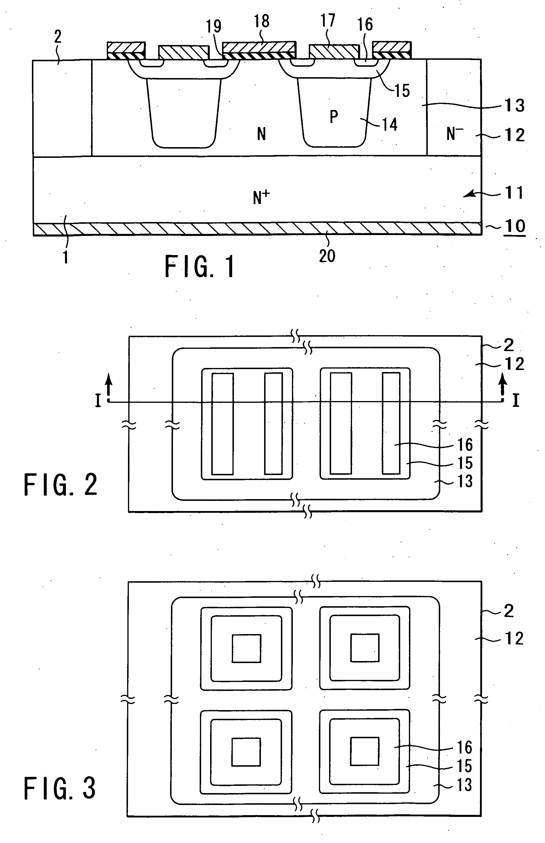
[0045]FIG. 1 is a diagram showing the sectional structure of a semiconductor device according to the first embodiment of the present invention. This semiconductor device is a vertical MISFET in which PN junctions are formed to extend in a depth direction. In each of the embodiments described below, for example, a first conductive type is N and, whereas a second conductive type is P.

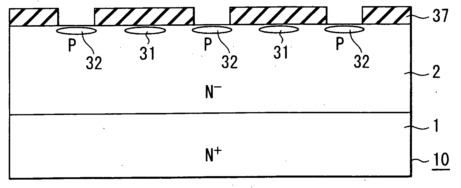
[0046] As shown in FIG. 1, a semiconductor substrate (layer) 10 consisting of, for example, silicon is composed of a first semiconductor substrate 1 and a second semiconductor substrate 2. The first semiconductor substrate 1 has impurities of a high concentration and an N type conductivity. The second semiconductor substrate 2 is formed on the first semiconductor substrate 1 and has an N type conductivity with an impurity concentration lower than that of the first semiconductor substrate 1. The second semiconductor substrate 2 m...

second embodiment

[0067] A second embodiment will be described with reference to FIGS. 13 to 20. In the first embodiment, the second semiconductor substrate 2 is composed of, for example, a single epitaxial growth layer or the like. In contrast, a semiconductor device according to the second embodiment has a structure in which the second semiconductor substrate 2 has a plurality of layers and in which PN junctions are formed to be deeper by repeating the manufacturing method of the first embodiment.

[0068]FIG. 13 shows the sectional structure of the semiconductor device according to the second embodiment of the present invention. This semiconductor device is a vertical MISFET in which PN junctions are formed to extend in the depth direction. In the second embodiment, the second semiconductor substrate 2 is composed of a plurality of epitaxial growth layers consisting of, for example, silicon. The first and second diffusion areas 13 and 14 are formed by forming a plurality of different impurity diffus...

third embodiment

[0082] A third embodiment will be described with reference to FIGS. 22 to 24. In addition the structure of the second embodiment, the third embodiment has a structure in which diffusion areas are further repeatedly formed breadthwise.

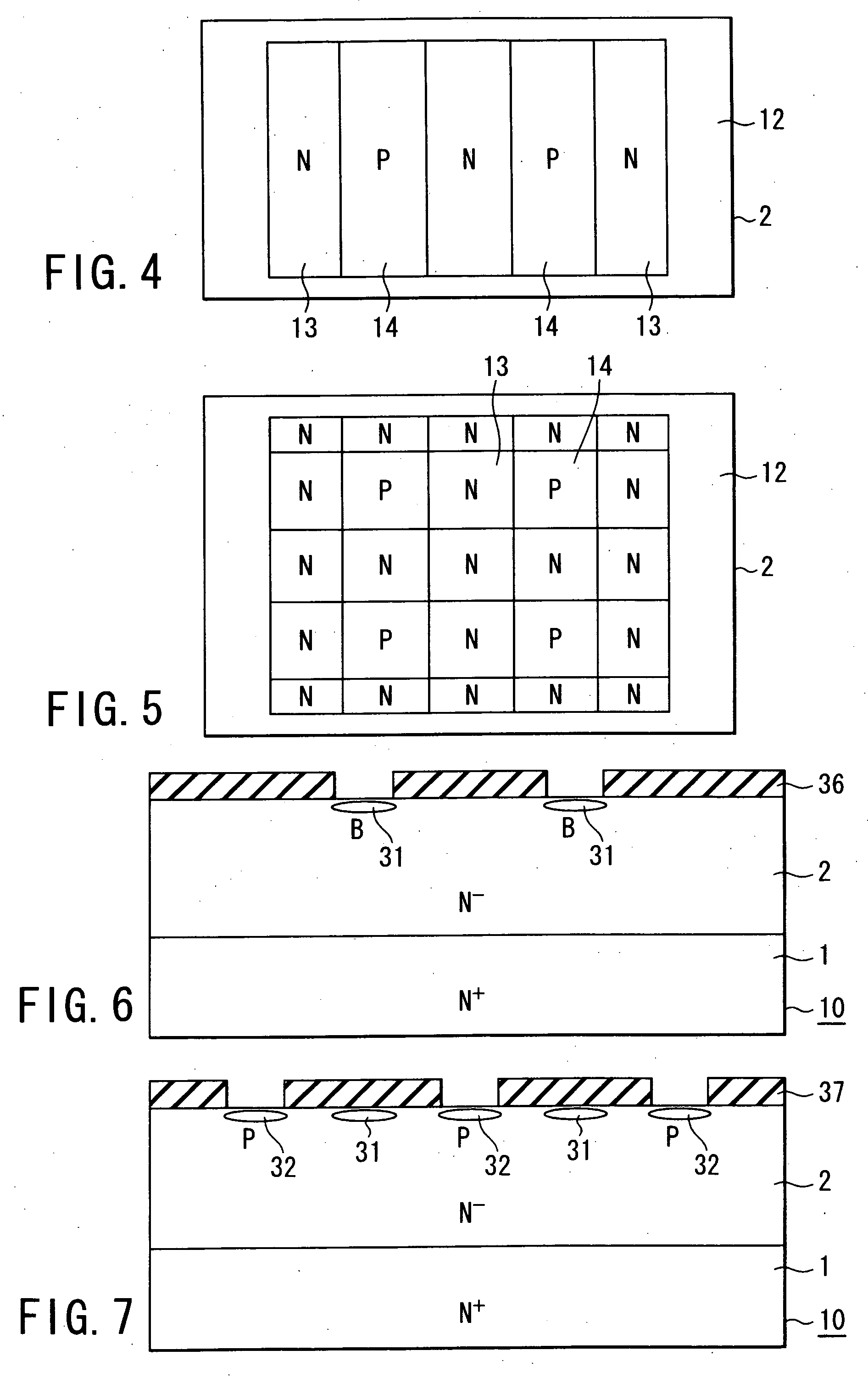
[0083]FIG. 22 shows the sectional structure of a semiconductor device according to the third embodiment of the present invention, i.e. the sectional structure of a semiconductor substrate provided with vertical MISFET elements. As shown in FIG. 22, for example, three second diffusion areas (P type areas) 14 are formed inside the semiconductor substrate 2 so as to be each sandwiched between the first diffusion areas (N type areas) 13. It is possible to further increase the number of second diffusion areas 14.

[0084]FIG. 23 shows an impurity concentration profile of a portion of the semiconductor device taken along the line XXIII-XXIII in FIG. 22. FIG. 24 shows a NET concentration profile indicating the total concentration distribution of the same portio...


PUM


Abstract

A semiconductor device includes a diffusion area formed in a semiconductor layer of a first conductive type. The diffusion area comprises first and second impurity diffusion areas of the first and second conductive types, respectively. The diffusion area has a first and second areas which are defined by an impurity concentration of the first and second impurity diffusion areas. A junction between the first and second area is formed in a portion in which the first and second impurity diffusion areas overlap each other. A period of the impurity concentration, in a planar direction of the semiconductor layer, of the first or second area is smaller than the maximum width, in the planar direction of the semiconductor layer, of the first and second impurity diffusion areas constituting the first or second area.

Description

CROSS-REFERENCE TO RELATED APPLICATIONS [0001] This application is based upon and claims the benefit of priority from the prior Japanese Patent Application No. 2001-395558, filed Dec. 27, 2001, the entire contents of which are incorporated herein by reference. BACKGROUND OF THE INVENTION [0002] 1. Field of the Invention [0003] The present invention relates to a substrate structure of a semiconductor device having vertical power MISFETs (Metal Insulator Field Effect Transistors) each having a gate electrode formed on a semiconductor substrate, as well as a method of manufacturing this substrate structure. [0004] 2. Description of the Related Art [0005] In a vertical power MIS (including a MOS (Metal Oxide Semiconductor) FET formed on a semiconductor substrate, a drain current flows between a source and drain electrodes formed on a top and bottom surfaces, respectively, of a semiconductor substrate. Such an element allows the resistance of a current passage to be reduced and is thus o...

Claims


Application Information

Patent Timeline
Patent Type & Authority Applications(United States)
IPC IPC(8): H01L29/00H01L21/425H01L21/336H01L29/06H01L29/08H01L29/78
CPCH01L29/0634H01L29/0696H01L29/0878H01L29/7802H01L29/7811
Inventor OKUMURA, HIDEKIKOBAYASHI, HITOSHITSUCHITANI, MASANOBUOSAWA, AKIHIKOSAITO, WATARUYAMAGUCHI, MASAKAZUOMURA, ICHIRO
Owner OKUMURA HIDEKI
Why Eureka
Try Eureka