Three dimensional package structure with semiconductor chip embedded in substrate and method for fabricating the same

Inactive Publication Date: 2006-07-06
PHOENIX PRECISION TECH CORP
View PDF3 Cites 195 Cited by
  • Summary
  • Abstract
  • Description
  • Claims
  • Application Information

AI Technical Summary

Benefits of technology

[0019] Therefore, the package structure in the present invention is fabricated by integrating chip-packaging and circuit-forming processes and combining carrier fabrication and package fabrication, thereby avoiding drawbacks in the conventional technology. The present invention also improves heat dissipating performance of the package structu

Problems solved by technology

If the heat cannot be dissipated timely, a semiconductor packages comprising the circuit board and the semiconductor chip may become overheated, thereby adversely affecting lifetime of the semiconductor chip.
At present, a ball grid array (BGA) package structure has failed to meet the requirements of electricity and heat dissipation in the case for high number of pins (over 1500 pins) and high frequency applications.
However, in the case of using a multi chip flip-chip package, not only the overall packaging costs are increased but also many techn

Method used


Image

  • Three dimensional package structure with semiconductor chip embedded in substrate and method for fabricating the same
  • Three dimensional package structure with semiconductor chip embedded in substrate and method for fabricating the same
  • Three dimensional package structure with semiconductor chip embedded in substrate and method for fabricating the same

Examples


Embodiment Construction

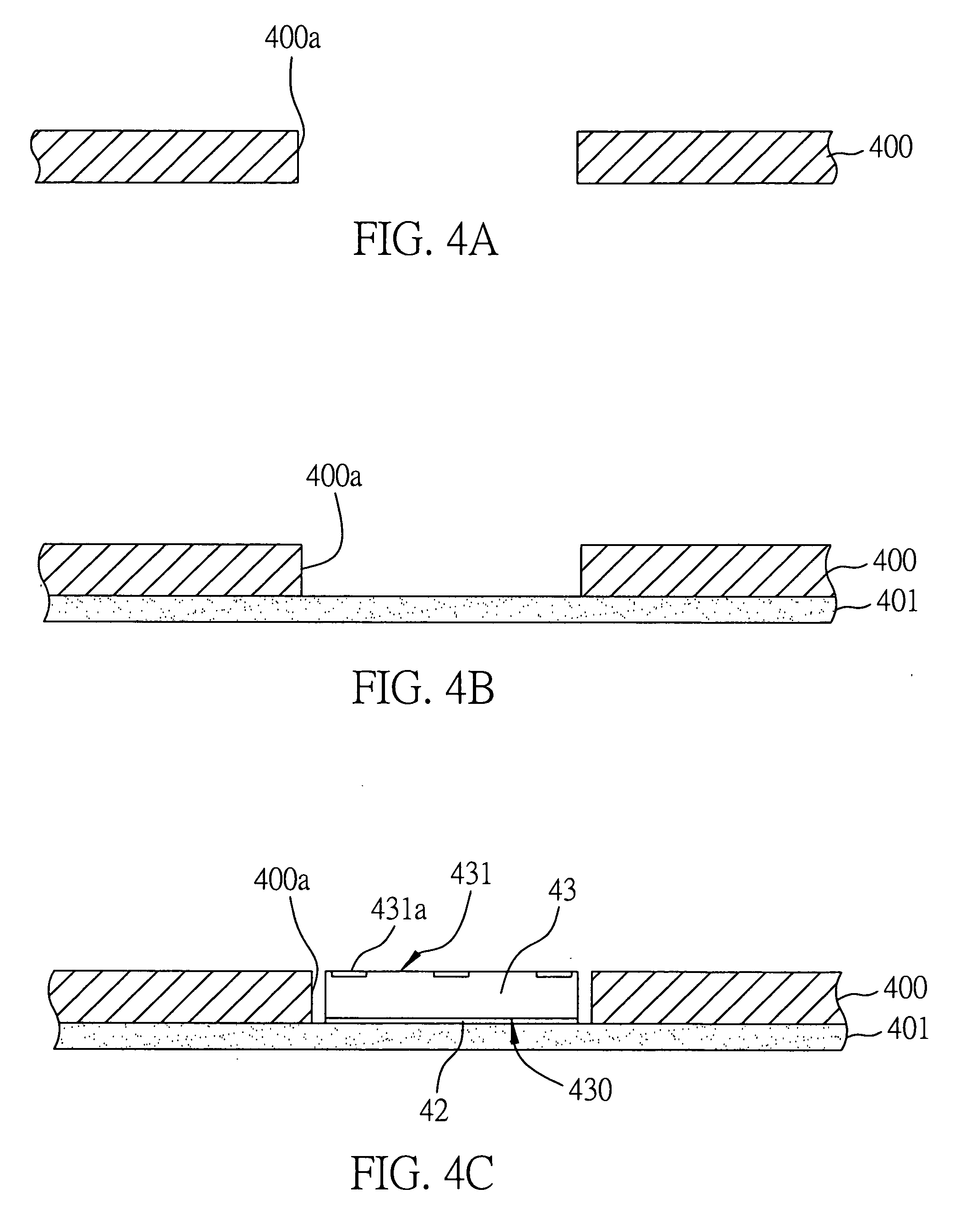
[0026]FIGS. 4A to 4F are cross-sectional views showing steps of a method for fabricating a package structure according to a first preferred embodiment of the present invention. It should be noted that all the drawings are simplified diagrams for only illustrating the basic architecture of the present invention. Thus, the drawings merely show components related to the present invention, and the shown components are not drawn according to practical numbers, shapes and size ratios. The numbers, shapes and size ratios of the components are selected according to design in practical implementation, and the component layout of the package structure may be more complex.

[0027] Referring to FIG. 4A, a carrier 400 with a cavity 400a is provided. The carrier 400 can be an insulating core plate, a metal plate, or a circuit board having circuits. A thickness of the carrier 400 may be determined according to a practical requirement.

[0028] Referring to FIG. 4B, subsequently the carrier 400 is mou...


PUM


Abstract

A three dimensional package structure with semiconductor chip embedded in substrate and a method for fabricating the same are proposed. A carrier with at least one cavity is mounted on a first insulating layer, and at least one semiconductor chip is mounted on the first insulating layer and received in the cavity of the carrier. A second insulating layer is formed on the carrier and the semiconductor chip. By performing a pressing process on both of the first insulating layer and the second insulating layer, a gap between the carrier and the semiconductor chip is filled. A circuit layer may be formed on the second insulating layer and is electrically connected to the semiconductor chip. Heat dissipating vias are formed in the first insulating layer and are connected to the semiconductor chip and a heat dissipating circuit so as to facilitate dissipation of heat generated from the semiconductor chip.

Description

FIELD OF THE INVENTION [0001] The present invention relates to three dimensional package structures with semiconductor chips being embedded in substrates and methods for fabricating the same, and more particularly, to a semiconductor package structure for integrating a semiconductor chip with a carrier, and a method for fabricating the semiconductor package structure. BACKGROUND OF THE INVENTION [0002] Along with development of electronic industry, it has endeavored to increasingly provide electronic products with multiple functions and high performances. To satisfy the high integration and miniaturization requirements for semiconductor packages, a circuit board for accommodating a plurality of active and passive components and providing circuit connections has accordingly been developed from a one-layer board to a multi-layer board so as to increase an available circuit area on the circuit board by means of interlayer connection technology to fulfill the requirement of integrated c...

Claims


Application Information

Patent Timeline
IPC IPC(8): H01L23/48H01L21/60H01L23/36H01L23/538H05K1/18H05K3/46
CPCH01L23/5389H01L2224/0401H01L24/20H01L24/24H01L2224/04105H01L2224/16225H01L2224/20H01L2224/211H01L2224/24227H01L2224/2518H01L2224/73267H01L2924/01029H01L2924/14H01L2924/15153H01L2924/15165H01L2924/1517H01L2924/15311H05K1/185H05K3/4602H05K2201/10674H01L24/19H01L2224/12105H01L24/25H01L2924/01033H01L2224/32225H01L2224/92144H01L2924/351H01L2924/00
Inventor HSU, SHIH-PING
Owner PHOENIX PRECISION TECH CORP
Why Eureka
Try Eureka