In-plane switching mode liquid crystal display device

a liquid crystal display and switching mode technology, applied in static indicating devices, non-linear optics, instruments, etc., can solve the problems of cross-talk and light leakage phenomena, structure degrades the aperture ratio of the lcd, and distorts the electric field, so as to prevent the degradation of picture quality and minimize parasitic capacitance

Active Publication Date: 2006-07-06
LG DISPLAY CO LTD
View PDF25 Cites 37 Cited by
  • Summary
  • Abstract
  • Description
  • Claims
  • Application Information

AI Technical Summary

Benefits of technology

[0019] An object of the present invention is to provide an in-plane switching mode liquid crystal display device that can prevent degradation of picture quality due to a signal interference of a data line by forming a rubbing direction perpendicular to the data line and disposing a common electrode and a pixel electrode according to the rubbing direction.
[0020] Another object of the present in

Problems solved by technology

Thus, a signal interference can be easily generated between the data line 10 and the pixel electrode 3, thereby causing a cross-talk and a light leakage phenomenon.
However, such an e

Method used


Image

  • In-plane switching mode liquid crystal display device
  • In-plane switching mode liquid crystal display device
  • In-plane switching mode liquid crystal display device

Examples


first embodiment

[0038]FIG. 3 is a plan view showing a unit pixel of a liquid crystal display (LCD) device in accordance with the present invention, while FIGS. 4A and 4B are cross-sectional views taken along lines II-II′ and III-III′ of FIG. 3.

[0039] As shown in FIG. 3, a liquid crystal panel includes a data line 100 and a gate line 101 arranged on a first substrate 110 (shown in FIGS. 4A and 4B) and defining a unit pixel region, a thin film transistor TFT as a switching device disposed at each crossing of the data line 100 and the gate line 101, and at least one pixel electrode 103 and a common electrode 105 alternately arranged in parallel to each other in the pixel region and generating an in-plane electric field.

[0040] In this case, though not shown, an alignment film rubbed in a direction perpendicular to the data line 100 is formed on the first substrate 110, and the pixel electrode 103 and the common electrode 105 are formed with a tilt angle within a range of about 0°˜45° in a direction pe...

second embodiment

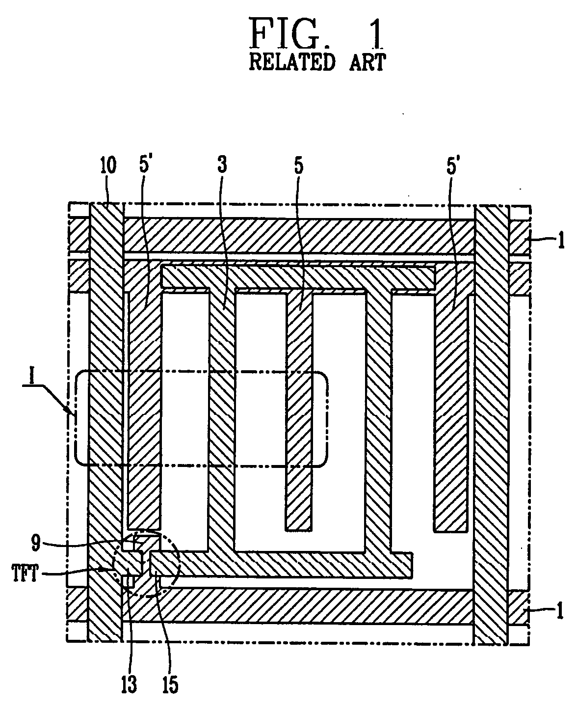
[0052] However, the LCD device has such shortcomings that a vertical dim phenomenon occurs due to parasitic capacitances generated among the pixel electrode, the pixel electrode line and the data line. Therefore, the present invention is directed to an IPS mode LCD capable of enhancing picture quality of the liquid crystal panel especially by removing the vertical line phenomenon.

[0053] The construction of the second embodiment is similar to that of the first embodiment, so only a different part and its effect will be described.

[0054] As illustrated, a liquid crystal panel includes a data line 200 and a gate line 201 arranged on a first substrate and defining a unit pixel region, a switching device TFT disposed at the crossing of the gate line 201 and the data line 200, and a plurality of pixel electrodes 203 and common electrodes 205 alternately arranged in parallel to each other in the pixel region and generating a in-plane electric field.

[0055] Although not shown in the drawing...

third embodiment

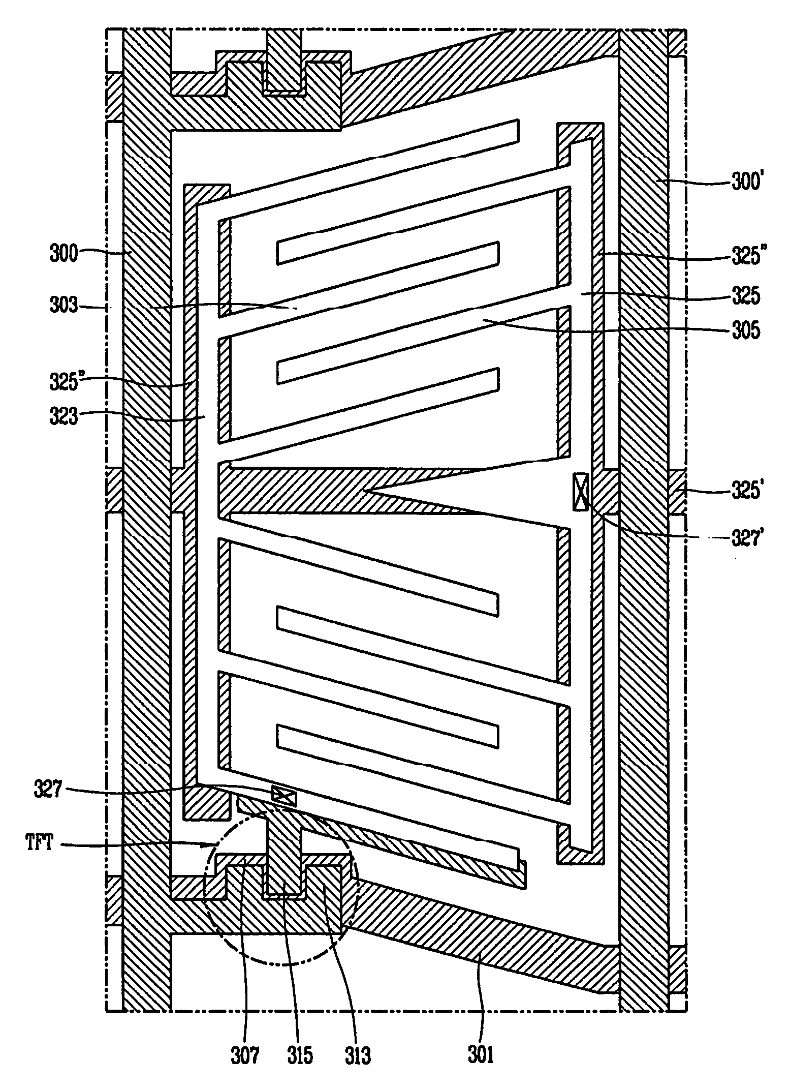
[0080] As shown in FIG. 10, a liquid crystal panel in accordance with the present invention includes a data line 300 and a gate line 301 arranged on a first substrate and defining a unit pixel region, a switching device TFT disposed at a crossing of the data line 300 and the gate line 301, and a plurality of pixel electrodes 303 and common electrodes 305 alternately arranged in parallel to each other in the pixel region and generating an in-plane electric field.

[0081] Although not shown in the drawing, an alignment film rubbed in a direction perpendicular to the data line 300 is coated on the first substrate, and the pixel electrodes 303 and the common electrodes 305 are formed to have a tilt angle in a range of 0°˜45° with respect to a direction perpendicular to the data line 300, thereby to correspond to the rubbing direction of the alignment film.

[0082] The switching device TFT includes a gate electrode 307 formed as a portion of the gate line 301, a semiconductor layer (not sho...


PUM


Abstract

An in-plane switching mode liquid crystal display device includes first and second substrates, a gate line on the first substrate, a data line crossing the gate line defining a unit pixel region, a thin film transistor at the crossing of the gate line and the data line, a pixel electrode line in parallel with the data line, a plurality of pixel electrodes formed to be protruded in an extended direction of the gate line from the pixel electrode line, a common electrode line adjacent to a data line of a neighboring pixel in the extended direction of the gate line and in parallel therewith, a plurality of common electrodes protruded from the common electrode line and alternately arranged in parallel with the plurality of pixel electrodes to generate an in-plane electric field, and a liquid crystal layer between the first and second substrates.

Description

[0001] The present invention claims the benefit of Korean Patent Application No. P2004-118352 filed in Korea on Dec. 31, 2004, which is hereby incorporated by reference. BACKGROUND OF THE INVENTION [0002] 1. Field of the Invention [0003] The present invention relates to a liquid crystal display (LCD) device, and more particularly, to an in-plane switching (IPS) mode LCD capable of preventing signal interference of a data line and reducing a vertical line deficiency. [0004] 2. Discussion of the Related Art [0005] Recently, as various mobile electronic devices including a mobile phone, a PDA or a notebook computer are being developed, demands for a light, thin, short and small flat panel display device which may be applied to the mobile electronic devices are increasing. Thus, researches for flat panel display devices such as a liquid crystal display (LCD), a plasma display panel (PDP), a field emission display (FED), and a vacuum fluorescent display (VFD) are actively ongoing. Among ...

Claims


Application Information

Patent Timeline
IPC IPC(8): G09G3/36G02F1/1343
CPCG02F1/133784G02F1/134363G02F1/136213G02F1/136227G09G3/3614G09G3/3648G09G2300/0434G09G2320/0209G02F1/1343
Inventor KIM, DO SUNGLEE, DO YOUNG
Owner LG DISPLAY CO LTD
Why Eureka
Try Eureka