Method and apparatus for controlling charge transfer in CMOS sensors with a graded transfer gate work function

a charge transfer and work function technology, applied in the field of image sensors, can solve problems such as signal loss of current images, and achieve the effects of low noise, high performance and low cos

Active Publication Date: 2006-07-06
RE SECURED NETWORKS LLC
View PDF13 Cites 13 Cited by
  • Summary
  • Abstract
  • Description
  • Claims
  • Application Information

AI Technical Summary

Benefits of technology

[0006] This innovation describes the process methods and process integration of an active pixel sensor that combines the advantages of both CCD and CMOS technologies. The low noise advantages of a true correlated multiple sampling pixel (e.g., Correlated Double Sample pixel) are created in a CMOS process with low cost and high performance with minimum impact on existing features and capabilities of the CMOS technology. Disclosed embodiments cover 4T pixel designs, although other protected embodiments cover 5T and other pixel designs.

Problems solved by technology

Otherwise, image lag causes signal loss for a current image and mixes the signals of the sequential images.

Method used


Image

  • Method and apparatus for controlling charge transfer in CMOS sensors with a graded transfer gate work function
  • Method and apparatus for controlling charge transfer in CMOS sensors with a graded transfer gate work function
  • Method and apparatus for controlling charge transfer in CMOS sensors with a graded transfer gate work function

Examples


Embodiment Construction

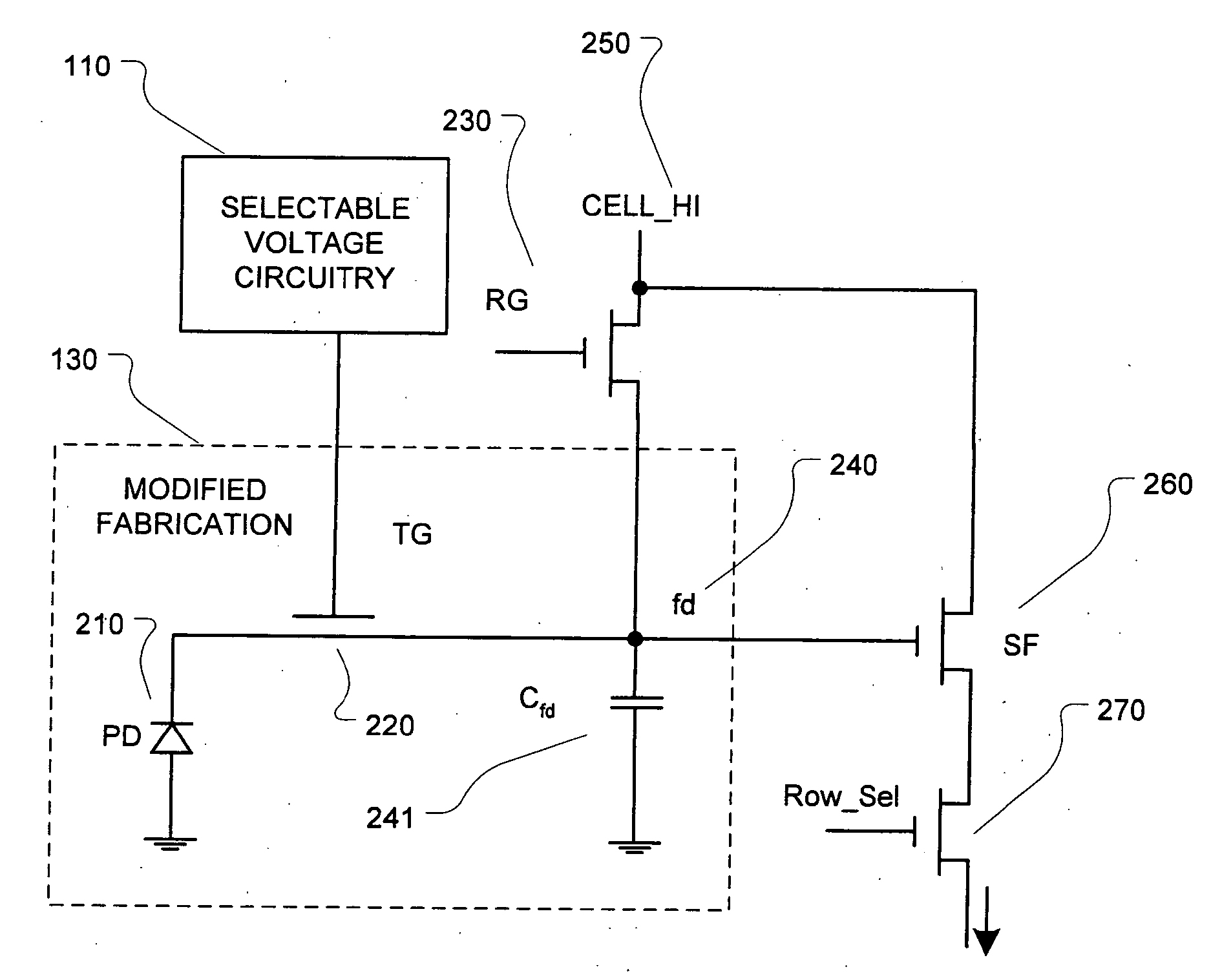
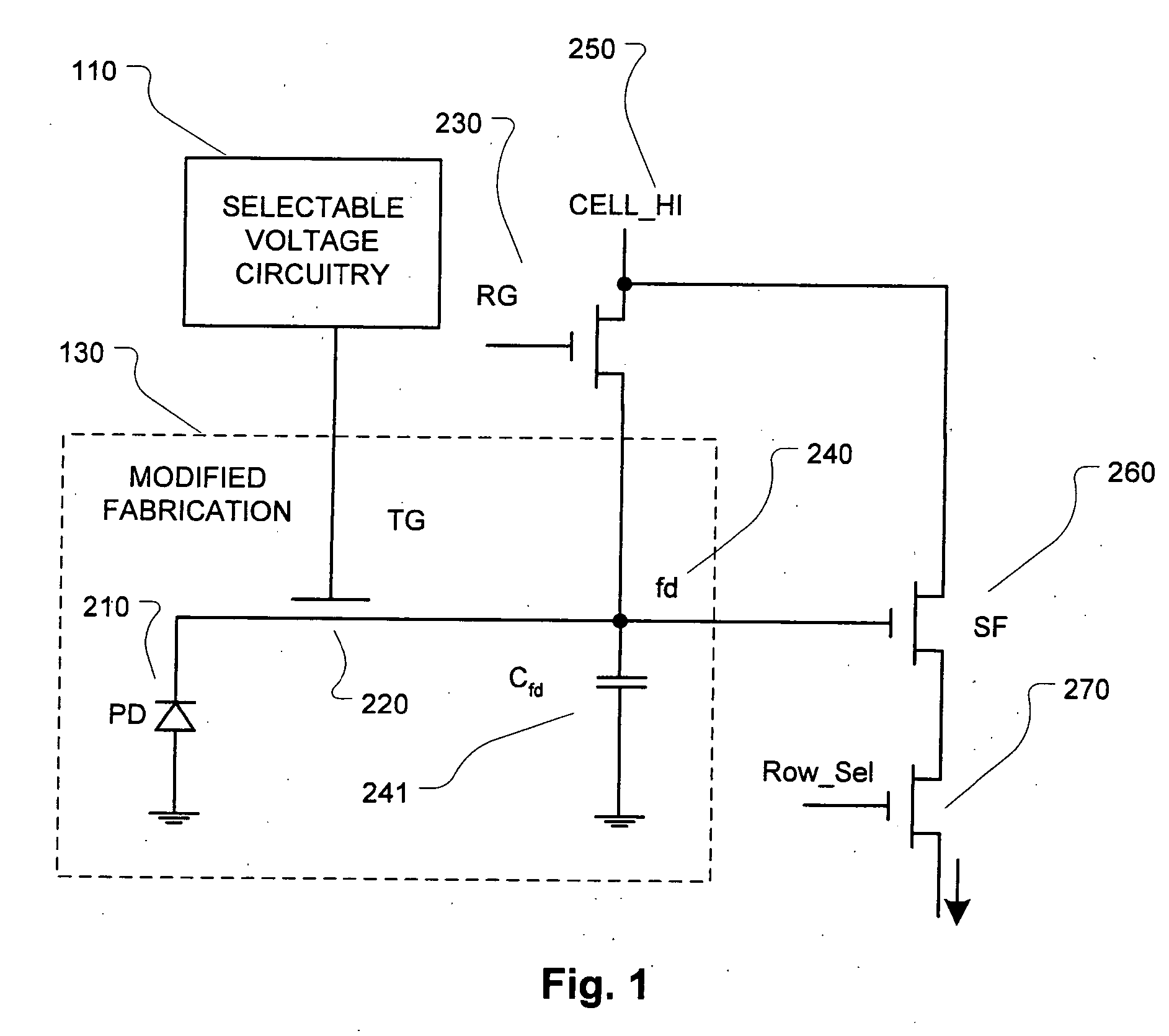
[0047] The pixel as illustrated in FIG. 1 is designed to overcome limitations of the CMOS process and achieve good picture quality levels that are comparable to CCD sensors.

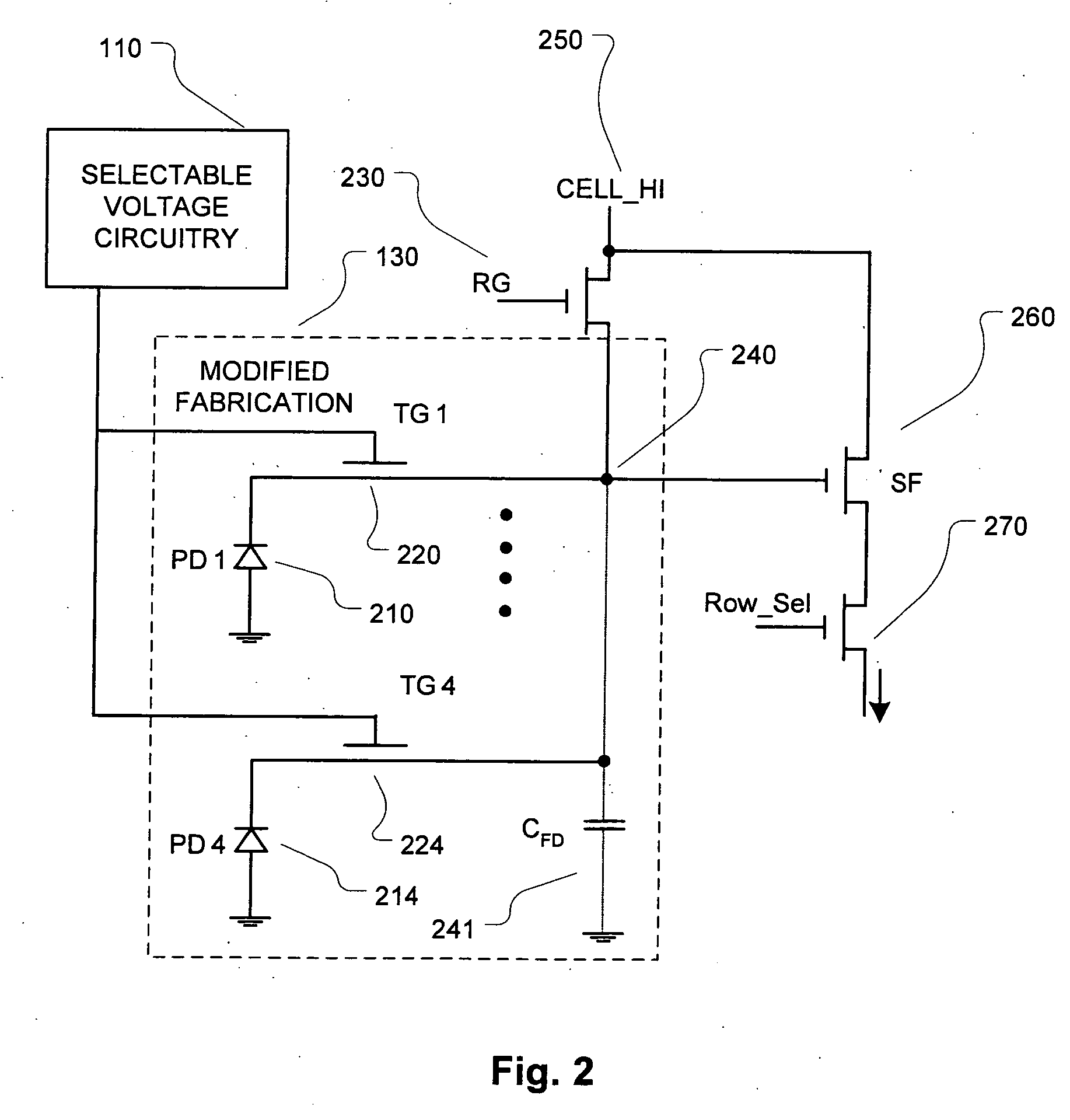
[0048] The pixel consists of a pinned photodiode (PD) 210 as light sensing element, a transfer gate (TG) 220, a floating diffusion 240 (and associated capacitance 241), a MOSFET as reset transistor 230, a second MOSFET as source follower 260, and a third MOSFET as row select transistor 270. The devices which have undergone modified fabrication 130 according to some embodiments include the pinned photodiode (PD) 210, the transfer gate (TG) 220, and the floating diffusion 240.

[0049] The pixel is designed to be built with the CMOS process with additional implantation steps to improve the performance. Only modest positive biasing voltages are required which can easily be provided by a CMOS process without the need for special high voltage devices. The process modifications are in the pixel array and therefore the r...


PUM


Abstract

An improved CMOS sensor integrated circuit is disclosed, along with methods of making the circuit and computer readable descriptions of the circuit.

Description

REFERENCE TO RELATED APPLICATION [0001] This application is related to the commonly owned U.S. patent applications Ser. No. 10 / ______, (HBES 1012-1), entitled “Method and Apparatus for Varying a CMOS Sensor Control Voltage”, by inventors Zeynep Toros, Richard Mann, Selim Bencuya, Sergi Lin and Jiafu Luo; to Ser. No. 10 / ______, (HBES 1013-1), entitled “Method and Apparatus for Removing Electrons from CMOS Sensor Photodetectors”, by inventors Zeynep Toros, Richard Mann and Selim Bencuya; to Ser. No. 10 / ______, (HBES 1014-1), entitled “Method and Apparatus for Controlling Charge Transfer in CMOS Sensors with an Implant by the Transfer Gate”, by inventors Toros et al.; to Ser. No. 10 / ______, (HBES 1015-1), entitled “Method and Apparatus for Controlling Charge Transfer in CMOS Sensors with a Transfer Gate Work Function”, by inventors Toros et al.; to Ser. No. 10 / ______, (HBES 1017-1), entitled “Method for Designing a CMOS Sensor”, by inventors Toros et al.; and to Ser. No. 10 / ______, (HB...

Claims


Application Information

Patent Timeline
Patent Type & Authority Applications(United States)
IPC IPC(8): H04N5/335
CPCH01L27/14609H01L27/14643H01L27/14654H01L27/14689H04N5/3575H04N5/3594H04N5/361H04N5/363H04N25/623H04N25/616H04N25/65H04N25/63
Inventor TOROS, ZEYNEPMANN, RICHARDBENCUYA, SELIM
Owner RE SECURED NETWORKS LLC
Why Eureka
Try Eureka