Image sensor with enlarged photo detection area and method for fabricating the same

a technology of image sensor and photo detection area, applied in the field of image sensor, can solve the problems of degrading image and reducing the amount of light, and achieve the effect of maximizing the photo detection area

Active Publication Date: 2006-07-06
INTELLECTUAL VENTURES II
View PDF10 Cites 152 Cited by
  • Summary
  • Abstract
  • Description
  • Claims
  • Application Information

AI Technical Summary

Benefits of technology

[0019] It is, therefore, an object of the present invention to provide an image sensor capable of...

Problems solved by technology

The decreased amount of the light increases image loss...

Method used


Image

  • Image sensor with enlarged photo detection area and method for fabricating the same
  • Image sensor with enlarged photo detection area and method for fabricating the same
  • Image sensor with enlarged photo detection area and method for fabricating the same

Examples


Embodiment Construction

[0027] Hereinafter, detailed descriptions of preferred embodiments of the present invention will be provided with reference to the accompanying drawings.

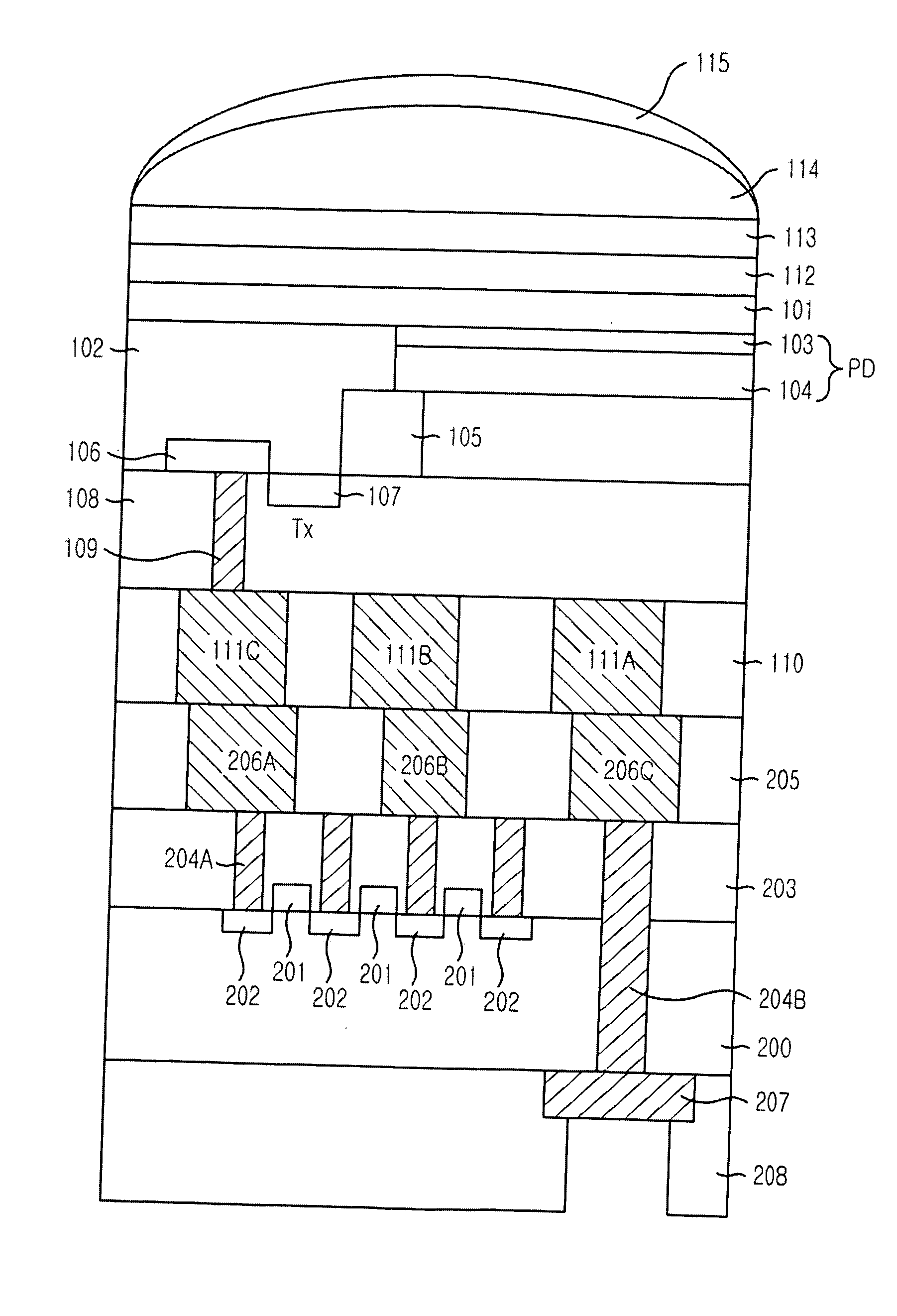
[0028]FIG. 3 is a cross-sectional view illustrating a unit pixel of an image sensor in accordance with a specific embodiment of the present invention.

[0029] The CMOS image sensor includes a third insulation layer 101 embodied in a silicon-on-insulator (SOI) structure; a color filter array (CFA) 112 provided on the third insulation layer 101; an over coating layer 113 provided on the color filter array 112; a microlens (ML) 114 formed on the over coating layer 113; a lens passivation layer 115 formed on the microlens 114; a photodiode PD formed with two different conductive regions 103 and 104 beneath the third insulation layer 101; an impurity region 105 contacted with the conductive region 104 which is a lower portion of the photodiode PD, i.e., a source region, and an impurity region 106 placed apart from the impurity region 105...


PUM


Abstract

A complementary metal oxide semiconductor (CMOS) device with a three dimensional integration structure and a method for fabricating the same are provided. An image sensor includes a first substrate in which a photo detection device is formed; a second substrate in which a peripheral circuit is formed, wherein the first substrate and the second substrate are bonded through a plurality of bonding pads formed on both the first substrate and the second substrate, and a back side of the first substrate is turned upside down; and a microlens formed on a top portion of the back side of the first substrate.

Description

FIELD OF THE INVENTION [0001] The present invention relates to an image sensor; and more particularly, to a complementary metal oxide semiconductor (CMOS) device with a three dimensional integration structure and a method for fabricating the same. DESCRIPTION OF RELATED ARTS [0002] Image sensors are semiconductor devices converting optical images into electrical signals. Among the image sensors, a charge coupled device (CCD) is a device which electric charge carriers are stored in and transferred to the capacitors as individual metal-oxide-silicon (MOS) capacitors are closely located with each other. [0003] Meanwhile, a complementary metal-oxide-silicon (CMOS) image sensor uses a CMOS technology using a control circuit and a signal processing circuit as a peripheral circuit. The CMOS image sensor adopts a switching method which makes MOS transistors as many as the number of pixels and uses the MOS transistors and thus, the CMOS image sensor sequentially detects an output. [0004]FIG....

Claims


Application Information

Patent Timeline
IPC IPC(8): G02F1/1335
CPCH01L27/14634H01L27/1464H01L27/1469H01L27/146H01L31/10
Inventor PARK, SANG-KYUN
Owner INTELLECTUAL VENTURES II
Why Eureka
Try Eureka