Electronic component package including heat spreading member

a technology of electronic components and heat spreading members, which is applied in the direction of power cables, cables, lighting and heating apparatuses, etc., can solve the problems of lsi chips, small camber of the substrate, and large expansion of the substrate, so as to improve the heat radiation and the effect of reliable heat transfer

Inactive Publication Date: 2006-07-06
FUJITSU LTD
View PDF44 Cites 6 Cited by
  • Summary
  • Abstract
  • Description
  • Claims
  • Application Information

AI Technical Summary

Benefits of technology

[0006] It is accordingly an object of the present invention to provide an electronic component package as well as an electronic component package assembly both capable of reliably transferring heat from an electronic component to a heat spreading member. It is also an object of the present invention to provide a printed circuit board unit greatly contributing to improvement of heat radiation from the electronic component package such as a LSI package.

Problems solved by technology

Such a substrate, however, tends to suffer from a larger expansion as compared with the LSI chip in response to a rise in temperature of the LSI chip, for example, because of the linear expansivity larger than that of the LSI chip.
This results in a slight camber of the substrate.
An efficient transfer of heat cannot thus be accomplished between the LSI chip and the heat spreader.

Method used


Image

  • Electronic component package including heat spreading member
  • Electronic component package including heat spreading member
  • Electronic component package including heat spreading member

Examples


Embodiment Construction

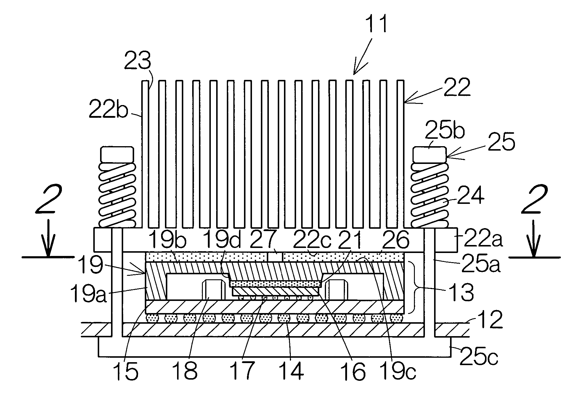
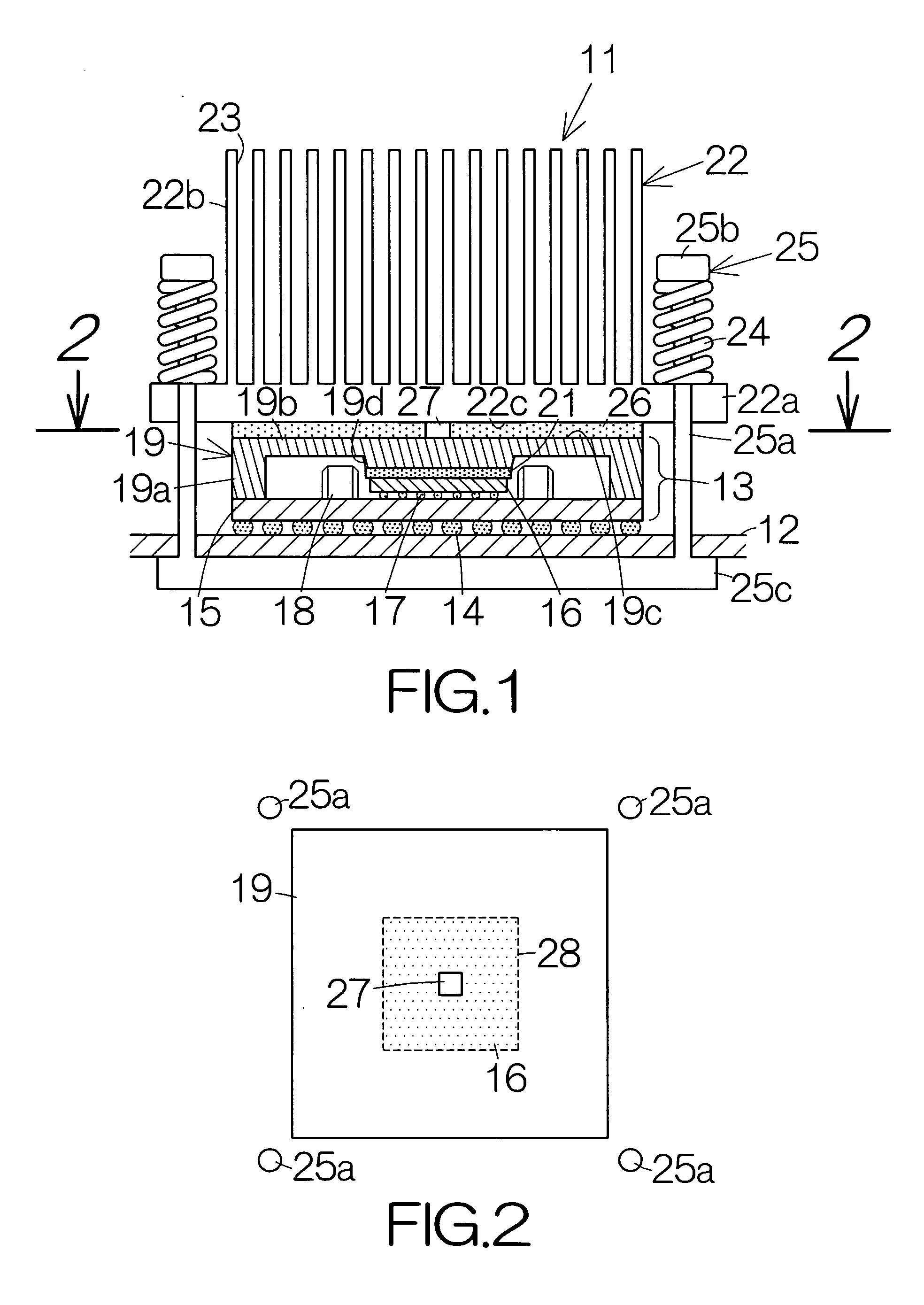
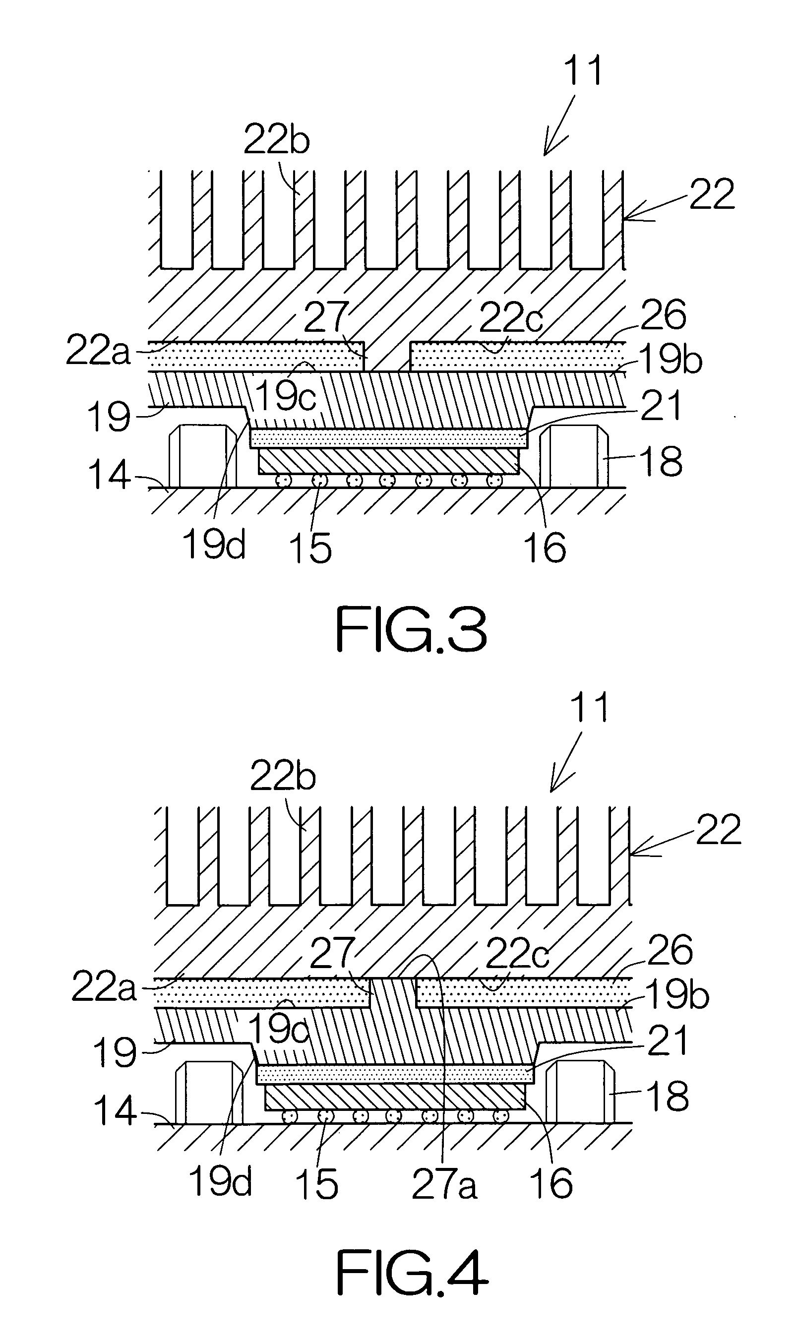
[0027]FIG. 1 schematically illustrates the structure of a printed circuit board unit 11 according to a first embodiment of the present invention. The printed circuit board unit 11 includes a printed wiring board 12. The printed wiring board 12 may includes a substrate made of a resin material. An electronic component package or LSI (Large-Scale Integrated circuit) package 13 is mounted on the printed wiring board 12. Terminal bumps 14 are employed to fix the LSI package 13 on the printed wiring board 12. The terminal bumps 14 may be made of an electrically-conductive material such as a solder material, for example.

[0028] The LSI package 13 includes a substrate 15 mounted on the front or upper surface of the printed wiring board 12. The substrate 15 may be made of a resin material, for example. An electronic component or LSI chip 16 is mounted on the front or upper surface of the substrate 15. Terminal bumps 17 are employed to fix the LSI chip 16 on the substrate 15. The terminal bu...


PUM


Abstract

A heat spreading member is received on a predetermined surface of an electronic component. The heat spreading member extends larger than the predetermined surface. A contact piece is contacted with the heat spreading member over a contact area smaller than the predetermined surface. The contact piece serves to realize concentration of an urging force applied to the heat spreading member. The heat spreading member is thus reliably urged against the electronic component. The concentration of the urging force serves to prevent the heat spreading member and the electronic component from camber even if heat is applied to the heat spreading member and the electronic component. Separation is thus avoided between the heat spreading member and the electronic component. The heat spreading member reliably keeps contacting with the electronic component, so that the electronic component package is allowed to enjoy improvement in heat radiation.

Description

BACKGROUND OF THE INVENTION [0001] 1. Field of the Invention [0002] The present invention relates to a printed circuit board unit including a printed wiring board and an electronic component package mounted on the printed wiring board. The electronic component package includes a heat spreading member covering over a predetermined surface of an electronic component such as a LSI (Large-Scale Integrated circuit) chip. The heat spreading member extends larger than the predetermined surface of the electronic component. [0003] 2. Description of the Prior Art [0004] A LSI package includes a LSI chip mounted on a small-sized printed wiring board. A heat spreading member or heat spreader is received on the upper surface of the LSI chip. A solidified material, such as a solidified silver paste, a solidified diamond paste, or the like, having heat conductivity is interposed between the LSI chip and the heat spreader. The solidified material serves to improve an efficient transfer of heat from...

Claims


Application Information

Patent Timeline
Patent Type & Authority Applications(United States)
IPC IPC(8): H05K7/20H01L23/04H01L23/367H01L23/40H01L23/42
CPCH01L23/04H01L23/3675H01L23/4006H01L23/42H01L2023/405H01L2023/4056H01L2023/4062H01L2023/4068H01L2023/4081H01L2224/16H01L2224/73253H01L2924/15311H01L2924/16152H01L2924/1616H01L2924/19105H01L2924/00011H01L2924/00014H01L2224/0401
Inventor KUBO, HIDEO
Owner FUJITSU LTD
Why Eureka
Try Eureka